Double helix turns up in new inorganic material!

Researchers at the Technical University of Munich (TUM) have synthesized an inorganic semiconductor material which features a double helix structure. This type of structure is best known as the carrier of genetic information in biological systems. The new material called SnIP is made up of tin, iodine and phosphorous and has novel optical and electronic properties, as well as great mechanical flexibility...
Researchers at the Technical University of Munich (TUM) have synthesized an inorganic semiconductor material which features a double helix structure. This type of structure is best known as the carrier of genetic information in biological systems. The new material called SnIP is made up of tin, iodine and phosphorous and has novel optical and electronic properties, as well as great mechanical flexibility.
Recent tests indicate that the new material has similar electrical characteristics to gallium arsenide but is far less toxic. The thinnest SnIP fibres produced to date consist of only five double helix strands and are only a few nanometres thick. According to Professor Nilges "Similar to carbon, where we have three-dimensional (3D) diamond, two dimensional graphene and one dimensional nanotubes, here we have, alongside the 3D semiconducting material silicon and the 2D material phosphorene, for the first time a one dimensional material – with perspectives that are every bit as exciting as carbon nanotubes."
Theoretical calculations indicate that this may just be the beginning; it could be that a whole range of further elements should form these kinds of inorganic double helices. Among its advantages Professor Nilges hopes that compared to organic solar cells, the new inorganic materials will be able to achieve significantly higher stability. For example, SnIP remains stable up to around 500°C (930 °F).
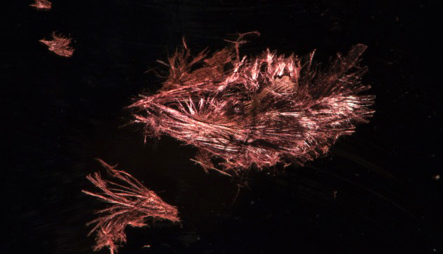
Just as in the organic chemistry equivalent the double helix strands of SnIP come in left and right-handed variants, materials that comprise only one of the two should have special optical characteristics. This makes them interesting for optoelectronics applications but so far, there is no technology available for separating the two variants. SnIP double helices can be suspended in solvents like toluene. In this way, thin layers can be produced easily and cost-effectively. The semiconducting property of SnIP will make it suitable for applications such as solar cells, temperature sensors and opto-electronics. The double helix arrangement of atoms forms fibres, up to a centimeter in length which can be split into thinner strands just a few nanometers thick. This could be a new raw material for future nanoelectronic applications.
