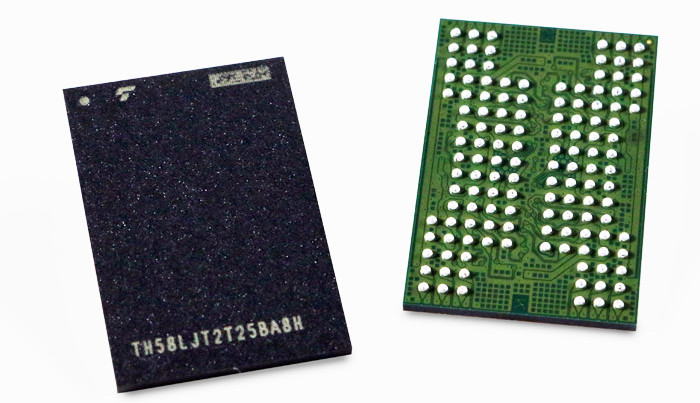
SSD Flash Memory Uses 112 Layers

The semiconductor manufacturer Kioxia and its partner Western Digital have announced a new generation of 3D NAND flash memory chips. Samples of this 512 Gbit TLC ‘5th generation’ BiCS5 3D NAND devices are available now, but full production volumes will not be rolling out until the second half of this year. Also in the pipeline are 1Tbit TLC and 1.33 Tbit QLC versions...
The semiconductor manufacturer Kioxia (a wholly owned subsidiary company of Toshiba Memory) and its partner Western Digital have announced a new generation of 3D NAND flash memory chips. Samples of this 512 Gbit TLC ‘5th generation’ BiCS5 3D NAND devices are available now, but full production volumes will not be rolling out until the second half of this year. Also in the pipeline are 1Tbit TLC and 1.33 Tbit QLC versions.
If the projected production timeline is accurate we should see SSDs with this technology reaching the marketplace before the start of next year.
Stack Them High
BiCS5 technology uses 112 layers compared to 96 used by the previous BiCS4 devices. Other refinements to the process have produced a significant increase in cell density horizontally which combined with 112 vertical layers achieves a bits-per-wafer density increase of up to 40% along with reduced production costs compared to the previous technology. The memory interface speed of this latest family of devices has also been boosted by 50%.If the projected production timeline is accurate we should see SSDs with this technology reaching the marketplace before the start of next year.
