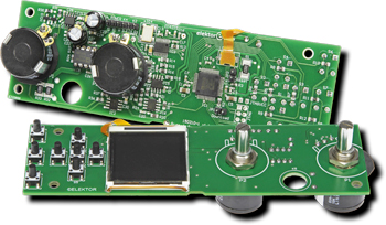
DDS Function Generator

Gerber file
CAM/CAD data for the PCB referred to in this article is available as a Gerber file. Elektor GREEN and GOLD members can exclusively download these files for free as part of their membership. Gerber files allow a PCB to be produced on an appropriate device available locally, or through an online PCB manufacturing service.
Elektor recommends the Elektor PCB Service service from its business partner Eurocircuits or AISLER as the best services for its own prototypes and volume production.
The use of our Gerber files is provided under a modified Creative Commons license. Creative Commons offers authors, scientists, educators and other creatives the freedom to handle their copyright in a more free way without losing their ownership.
Extra info / Update
Direct Digital Synthesis (DDS) with analog front-end
Frequency range: 1 – 10 MHz
Frequency resolution: 0.28 Hz
Output: 0 – 15 Vpp
THD+N (100 kOhm load, B > 500 kHz):
1 V, 1 kHz: 0.12% (0.09% for B = 22 kHz)
5 V, 1 kHz: 0.1% (0.09% for B = 22 kHz)
1 V, 10 kHz: 0.1% (0.09% for B = 80 kHz)
5 V, 10 kHz: 0.09% (0.08% for B = 80 kHz)
1 V, 100 kHz: 0.1%
5 V, 100 kHz: 0.08%
S/N (referred to 1 V): 72 dB
Maximum output (10 MOhm load):
Sine: 16 Vpp
Triangle: 16 Vpp
Square: 18 Vpp
DC offset voltage range: –10 to +10 V
Output impedance: 50 Ohm
Duty cycle (square wave): 1 – 99%
Rise and fall time (80%, square wave): 100 ns
Sweep mode
Power consumption: 3 VA
Visit www.elektor-labs.com/150210 for more figures and plots.
Components
The BOM (Bill of Materials) is the technically exhaustive listing of parts and other hardware items used to produce the working and tested prototype of any Elektor Labs project. The BOM file contains deeper information than the Component List published for the same project in Elektor Magazine. If required the BOM gets updated directly by our lab engineers. As a reader, you can download the list here.
Want to learn more about our BOM list? Read the BOM list article for extra information.
Component list
Generator Board
Resistors
All 1%, 0.125 W, SMD 0805
R1 = 220Ohm, 1%, 0.75W, SMD 2010
R2,R22,R23,R37 = 1kOhm
R3 = 1kOhm, 1%, 0.1W, SMD 0603
R5,R6,R7,R8,R9,R10,R11,R12,R30,R31,R36 = 10kOhm
R13 = 6.8kOhm
R14, R15 = 200Ohm
R16, R19, R25 = 910Ohm
R17, R20 = 1.2kOhm
R18, R26 = 2.0kOhm
R21, R24 = 499kOhm
R27 = 220Ohm
R28 = 10Ohm
R29 = 10kOhm, 1%, 0.1W, SMD 0603
R32, R33 = 100Ohm, 1%, 0.75W, SMD 2010
P1 = 10kOhm, 2W, 10-turn potentiometer
P2 = 1kOhm, 2W, 10-turn potentiometer
Capacitors
Default: SMD 0603
C1,C3,C4,C12,C13,C14,C16,C17,C19,C20,C26,C27,C28,C29,C31 = 100nF, 50V, X7R
C2, C5 = 10µF, 16V, X7R, SMD 1206
C6, C7 = 470nF, 25V, X7R
C11 = 1µF, 16V, X7R, SMD 1206
C15 = 10nF, 50V, X7R
C18 = 10pF, 50V, C0G/NP0
C21 = 100pF, 100V, C0G/NP0, SMD 0805
C22, C23 = 220µF, 25V, radial, 3.5mm pitch, diam. 8mm max.
C24, C30 = 100nF, 50V, X7R, SMD 0805
Semiconductors
IC1 = ADUC7024BSTZ62, LQFP-64, programmed*
IC2 = AD8032ARZ, SOIC-8
IC3 = AD9834BRUZ, TSSOP-20
IC4 = FXO-HC736R-75, 7 x 5 mm
IC5, IC6 = AD8042ARZ, SOIC-8
IC7 = ADG779BKSG-REEL7, 6-Lead SC-70
IC8 = AD811ANZ, DIP-8
IC9 = OP1177ARZ, SOIC-8
IC10, IC11 = ADR1581ARTZ-REEL7, SOT-23-3
Other
K1 = Socket, 0.5 mm, 1.5 mm stack, 10-way, DF23C-10DS-0.5V(51), Hirose (HRS)
K2, JP1, JP2 = 1x2 pin header, vertical, 0.1’’ pitch
K3 = 2x3 pin header, vertical, 0.1’’ pitch
K4 = 1x4 pin header, vertical, 0.1’’ pitch
K5 = BNC 50 Ohm, Straight Bulkhead Jack, Panel mount
S1-S8 = 6 mm tactile switch, actuator length 4.9mm, 24V/0.05A, SPST-NO
8-way DIP socket for IC8,
Graphic B/W replacement LCD for Nokia 6100
Miscellaneous
Aluminum enclosure, Hammond type 1455T1601, 165 x 160 x 51.5mm
Optional: EMI/EMC filter, inlet, IEC, 250VAC / 4A
2 knobs, black, 16mm, 0.25 in. shaft diam.
PCB 150210-1 v1.11 (www.elektor.com)
* Not available ready programmed from www.elektor.com
Component List
Power Supply
Resistors (1%, 0.6 W)
R1, R3 = 180Ohm
R2, R4 = 2.0kOhm
R5 = 240Ohm
R6 = 390Ohm
R7 = 10kOhm, 5%, 0.25W
Capacitors
C1,C2,C3,C4,C15,C16 = 10nF 50V, Y5V, 0.2’’ pitch
C5 = 1000µF 50V, 5 or 7.5 mm pitch, 16mm diam.
C6 = 470µF 50V, 5 or 7.5mm pitch, 13mm diam.
C7,C8,C13,C14,C18,C21 = 100nF 50V, X7R, 0.2’’ pitch
C9,C10,C11,C12,C19,C20 = 10µF 50V, 2mm pitch, 6.3mm diam. max.
C17 = 47µF 50V, 2.5mm or 3.5mm pitch, 8mm diam. max.
Semiconductors
D1,D2 = STPS2L60, DO-41 case
D3,D4,D5,D6 = 1N4007, DO-41 case
IC1,IC3 = LM317, TO-220 case
IC2 = LM337, TO-220 case
LED1 = LED, green, 3mm
Miscellaneous
K1 = 2-way PCB screw terminal block, 0.3’’ pitch, 500V
K2 = 4-way (2x2) PCB screw terminal block, 0.2’’ pitch, 250V
TR1 = 2x115V prim./2x15V sec., 10VA, e.g. Block FL 10/15
F1 = fuse, 100 mA (230 VAC line) or 200mA (115 VAC line); slow blow, 250V, 20 x 5mm
F2, F3 = fuse, 315mA, slow blow, 250V, 20x5mm
Fuse holder for F1, F2, F3, 20 x 5mm, 500V, 10A
Covers for F1, F2, F3 fuse holders, 20 x 5mm
JP1 = Jumper wire
PCB 150210-2 v1.1 (www.elektor.com)


Discussion (0 comments)