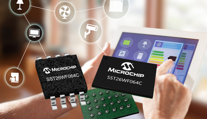
Low-voltage 64-Megabit Serial Quad I/O™ SuperFlash® memory from Microchip improves power consumption in battery-powered devices
September 05, 2017
on
on

Key Facts:
- SST26WF064C outputs data on both edges of the clock to reduce overall data access time
- SuperFlash technology reduces power consumption with the industry’s fastest erase times
- Features hardware-controlled device reset and Execute-in-Place (XIP) with no code shadowing
- Boosts performance in standard form factors with a 4-bit multiplexed I/O serial interface
Microchip announces availability of a new 1.8V Serial Quad I/O™ SuperFlash® memory device. The SST26WF064C, a low-voltage 64-Megabit device, combines Dual Transfer Rate (DTR) with proprietary SuperFlash NOR Flash technology, making it ideal for wireless and battery-powered applications. DTR gives customers the ability to output data on both edges of the clock which reduces overall data access time and power consumption. SuperFlash technology also reduces power consumption by providing the industry’s fastest erase times. Typical chip-erase time for the SST26WF064C is between 35 and 50 milliseconds, compared to competitive Flash devices which take more than 30 seconds to erase.
The SST26WF064C also integrates a hardware-controlled reset functionality enabling a robust device reset. Most serial Flash devices in the market do not support hardware reset function due to pin-count limitations on the package. With this Microchip device, customers have the option to reconfigure the HOLD# pin for this reset function.
Operating at frequencies reaching 104 MHz, the device enables minimum latency eXecute-In-Place (XIP) capability without the need for code shadowing on Static Random Access Memory (SRAM). The new device uses a 4-bit multiplexed I/O serial interface to boost performance while maintaining the compact form factor of standard serial Flash devices. The SST26WF064C also supports full command-set compatibility with traditional Serial Peripheral Interface (SPI) protocol.
Microchip’s high-performance SuperFlash technology also means the device is based on a proprietary split-gate Flash memory cell giving additional capabilities such as high endurance cycling of up to 100,000 erase/write cycles, data retention of over 100 years and the industry’s fastest erase times.
Developers can begin designing with the SST26WF064C Flash memory today using Verilog and IBIS models as well as device drivers.
The SST26WF064C is offered in a variety of package options including an 8-contact WDFN (6 mm x 5 mm), 8-lead SOIJ (5.28 mm), 16-lead SOIC (7.50 mm) and 24-ball TBGA (8 mm x 6 mm).
For more information, visit Microchip’s Web site at: www.microchip.com/SST26WF064C
Read full article
Hide full article


Discussion (0 comments)