One device is PIN diode, MOSFET or BJT
June 19, 2017
on
on

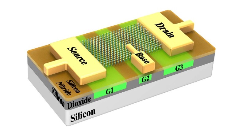
Researchers at SUNY-Polytechnic Institute in Albany, New York claim to have made a reconfigurable device that can be a p-n diode, a MOSFET or a BJT. Researcher Ji Ung Lee said “we can form a single device that can perform the functions of all three devices”.
The device is made of 2-D tungsten diselenide (WSe2), a new transition metal dichalcogenide semiconductor. This class of materials is promising for electronics applications because the bandgap is tunable by controlling the thickness, and it is a direct bandgap in single layer form.
The bandgap is one of the advantages of 2D transition metal dichalcogenides over graphene, which has zero bandgap.
In order to integrate multiple functions into a single device, the researchers developed a new doping technique. Before the discovery of WSe2 for the new application there was a lack of doping techniques. Through doping, the researchers could realize properties such as ambipolar conduction, which is the ability to conduct both electrons and holes under different conditions.
The doping technique also means that all three of the functionalities are surface-conducting devices, which offers a single, straightforward way of evaluating their performance.
The researchers plan to build complex ICs using fewer device elements than CMOS. “This will demonstrate the scalability of our device for the post-CMOS era,” Lee said.
Read full article
Hide full article


Discussion (0 comments)