

Error Analysis: Triple-Check Footprints Twice
July 20, 2021
on
on
To avoid footprint mistakes, one of the most common pitfalls of PCB design, board designers tend to rely on footprint libraries provided by component suppliers. They know what they are doing, right? As Nice, France-based engineer Stéphane Perez explains, it always helps to check footprints!
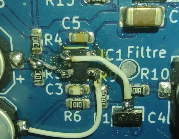
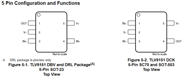
"However, after powering up the board, it did not work. No matter what we tried, it just wouldn’t work. Several hours of searching later and having replaced almost every part, I went back to the datasheet to see if I had missed something. And what do you know? The component footprint was for the TLV9151IDCKR! (Similar package, but some pins are swapped.) As I write this, this part is available for sale, but it wasn’t at the time of prototyping. After rewiring and correcting the board, the prototype could be validated," Perez added.
Perez concludes with the following advice:
"Despite more than 10 years of experience, I had never had to question so-called public component libraries. But now I always check the footprints of the circuits I use twice, especially when they are new and even more so if they have variants. And when I have the time, I design them myself. That way if there is a mistake, I know who to blame. Footprint designers make mistakes too!"
Check Footprints
According to Perez, "When we develop a new product, we try to use recent or new components to ensure the durability of the design. Being used to sourcing, I looked for a good quality op-amp for a simple microphone amplifier and found the TLV9151IDBVR (note the DBV part in the reference). To save time when routing the circuit board in Kicad, I usually use libraries available on the Internet and especially those provided by my usual supplier. The PCB was ordered and assembled immediately after receiving it.""However, after powering up the board, it did not work. No matter what we tried, it just wouldn’t work. Several hours of searching later and having replaced almost every part, I went back to the datasheet to see if I had missed something. And what do you know? The component footprint was for the TLV9151IDCKR! (Similar package, but some pins are swapped.) As I write this, this part is available for sale, but it wasn’t at the time of prototyping. After rewiring and correcting the board, the prototype could be validated," Perez added.
Perez concludes with the following advice:
"Despite more than 10 years of experience, I had never had to question so-called public component libraries. But now I always check the footprints of the circuits I use twice, especially when they are new and even more so if they have variants. And when I have the time, I design them myself. That way if there is a mistake, I know who to blame. Footprint designers make mistakes too!"
More on PCBs, Footprints and PCB Design
Want to learn more? Consider these resources:- C. Abate, "DIY PCB Printing with the Voltera V-One and GreatScott," ElektorMagazine.com, 2/1/2021.
- C. Valens, "How-To: Design a PCB with KiCAD EDA," ElektorMagazine.com, 7/19/2021.
- S. Drimer, "Circuit Shorts: PCB Fasteners," ElektorMagazine.com, 3/31/2021.
Read full article
Hide full article
Discussion (1 comment)
SteveMJ 3 years ago
I have had the misfortune of using one manufacturer’s connector for schematic design and what I thought was the same manufacturer’s connector for board layout. There was big difference; one connector’s pin-out ran 1,2, 3… along one side, the other (mechanical equivalent) connector was 1, 3, 5… along one side and 2,4,6… along the other.
Upon investigation, (after finding the circuit did not integrate to the remainder of the system due to incorrect connections) I found that the manufacturers for the footprint defined connector had bought out another company that was a second source for the schematic connector and their libraries were at odds! This meant that pin 1 on both schematic and layout were correct all the others were wrong.
The design reviews had checked all the connections were correct; pin 2 to pin 2 etc.