HDI in the Middle
on
A New Cost-Effective PCB Pooling Service for Tiny BGAs
Sometimes there’s a part that we really want to use, but it’s only available in a fine-pitch BGA package — using it will tip our design over the ‘standard PCB technology’ line into HDI territory. HDI technically means high-density interconnect, and practically means that we’re able to design with smaller clearances and thinner tracks. And, we’re able to use ‘microvias’: vias with smaller pads and smaller hole diameters than what is normally possible with mechanical drilling.

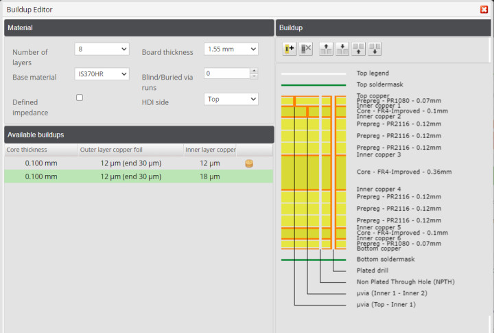
HDI enables miniaturization, which is great, but it may be annoying if it is ‘forced’ on us from a single tiny component onto the entire board, which then becomes prohibitively expensive. At Eurocircuits, we have the solution ‘in the middle’ that can help our customers deal with both the annoyance and the cost. Our HDI pool (Figure 1), an 8-layer buildup, keeps the ‘standard technology’ pattern classifications as they are, and adds microvias between layers 1–2 and 2–3 or 8–7 and 7–6, but not both. This lets our customers design with those fine-pitch BGAs, where cost is manageable since the HDI is limited to only a small area and to two microvia ‘runs’.
In Practice
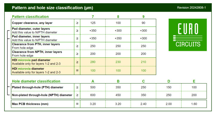
What does this mean in practice? Let’s look at Pattern Class 7 with Drill Class E from Figure 2, where the smallest pad diameter possible is 0.45 mm (0.1 + 0.35 mm); that won’t fit inside most fine pitch BGA pad diameters. However, when we use the same classification together with the HDI pool, the smallest diameter becomes 0.28 mm, which will fit! This allows designers to place vias in the centre of BGA pads without needing to enlarge the pads beyond the manufacturer’s recommendations. The smaller microvia pads also mean that using dogbone patterns becomes a possibility.

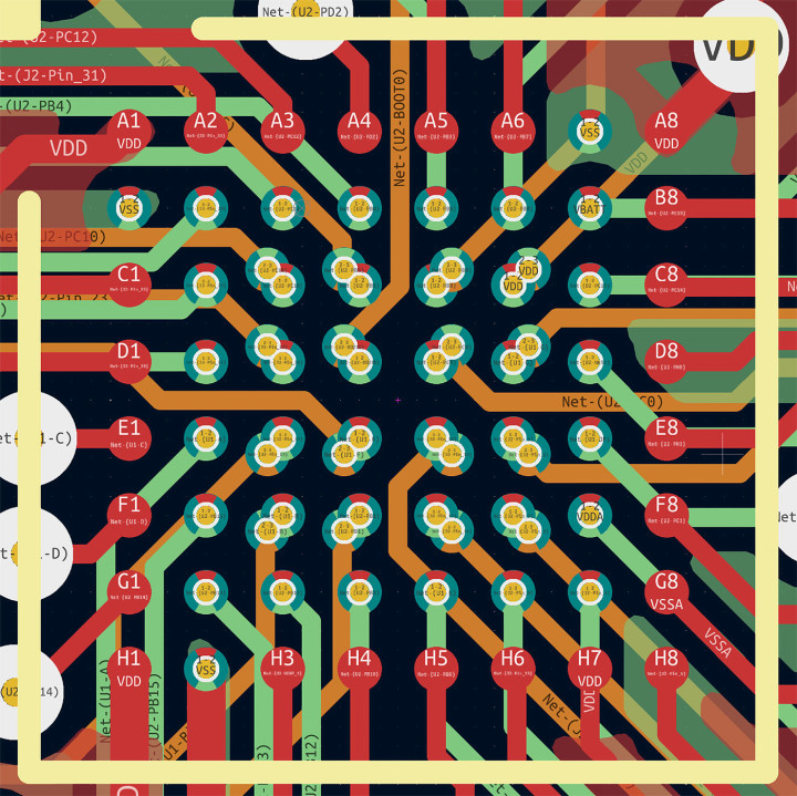
Obviously, it’s impossible to cover all BGA pin arrays and their pin configurations in order to determine which part will be routable and which won’t. However, we have configured our pool parameters such that full 8×8 arrays should be fully routable for BGAs down to 0.4 mm pitch. (Figure 3 shows an example of a fully fanned-out 8×8 0.4 mm pitch part.) But of course, larger arrays are possible too, and it all depends on the array size, pin configuration, and how those pins are used. In many packages, there are No Connect pins, and in most designs not all pins of a microcontroller or processor are used, which may ease routing-out large BGA arrays with only two microvia ‘runs’.
What now? We invite you to upload your designs to our Visualizer and check them for manufacturability. As always, we welcome your feedback on how this service may solve your manufacturing issues.


Discussion (1 comment)
webci 4 months ago