
Photovoltaic Basics (Part 1): Know Your PV Panels for Maximum Efficiency
on
Getting electricity from the sun in the way that best suits your needs requires knowledge of photovoltaic technologies and appropriate use of the elements of a system. In this article — published in two parts — we start with an overview of the structure, the physical and electrical features of different panel types available on the market.
Among all renewable energy sources, the one that we perceive to be closest to us, affordable and so scalable that it can be used as much on a mobile device as in vast solar parks, is photovoltaics; it is no coincidence that it is the most incentivized even at the level of small domestic installations alone.
Just in the context of the individual home, the energy restrictions resulting from the 2022 supply crisis saw the light of regulatory interventions in favor of the implementation of “balcony photovoltaics”, consisting of the installation of even a 200…300 W panel on the balustrade, which combined with an inverter could provide a 230-V AC source of electricity, added to that of the electricity grid to limit the withdrawal from the latter or make up for short blackouts.
When used offline, which is also an option for such a small solar plant, this solution could then be considered as a variant of the so-called “stand-alone photovoltaic”. This is a system, which can have a power of even a few kW, but which operates independently providing 230 V AC/50Hz electricity, thanks to an inverter that is not synchronized with the grid frequency and is not directly connected to the household grid.
In these pages, we will give an overview of the component elements of a typical photovoltaic system; in the next installment, we’ll then come to examples of stand-alone solutions that can be integrated with the electricity grid, even with grid feed-in.
The Photovoltaic Panel
In a system for generating electricity from the sun, the key element is the photovoltaic panel, since it is the one that physically converts solar energy into electricity; the rest is pure electronics, broken down into switch, battery charger and power inverter.
The sun sends an average of 1,367 W per m² to the Earth’s atmosphere, which corresponds to more than 50 million GW delivered to our planet: about 10,000 times the needs of the entire world population. It is, therefore, a matter of getting the most out of this energy.
How much electricity can be derived from a photovoltaic system, and under what conditions, depends strictly on the solar panel. For this reason, research is directed mainly toward three goals: improving conversion efficiency (i.e., more electric watts at the same irradiance), increasing the usable angle from which to receive the sun’s rays, and increasing panel durability.
Another key factor is the cost of production of photovoltaic panels from which comes the cost of the electricity produced, which, although it also depends on efficiency, is not solely related to it.
Certainly, today’s prices are competitive, which, net of incentives, makes the cost per watt produced comparable to that of traditional energy sources; in fact, if a decade ago, the cost of installed power was 5…6 €/W, today it has fallen below 1 €/W.
The photovoltaic panel converts into electricity the energy of the solar radiation impinging on its surface, thanks to the energy it possesses, which is directly proportional to frequency and inversely to wavelength: this means that the energy of infrared is less than that of ultraviolet for the same amount of irradiation.
In a photovoltaic panel, electrical energy is obtained by photovoltaic effect from elementary structures called photovoltaic cells; each cell is a PN-junction semiconductor diode constructed so that the junction is exposed to light and unpolarized. In the PN junction, the P side is abundant with atoms of trivalent elements and the N side is rich in pentavalent impurities; therefore, on the P side the junction has a shortage of electrons, which are instead in excess on the N side.
When the photons forming the light invest a PN junction — more specifically the surface of the trivalent doping region (P) — they determine a potential difference due to the photovoltaic effect, since each photon that invests a dopant atom frees an electron, which comes out of its bond and becomes available for conduction. In photovoltaic cells, light can reach the PN junction because the N layer is extremely thin, such that it is transparent.
If the junction is not connected to anything, the electrons recombine, releasing their energy in the form of heat, but if you connect the ends of the junction to a user, they flow into it resulting in electric current, and then re-enter the junction from the P side and recombine.
The photovoltaic effect can be observed in the fourth quadrant of the characteristic curve of the PN-junction diode. The phenomenon occurs provided that the light radiation has a wavelength such that the energy of the photons is sufficient to overcome that required to free the electrons from their bonds; this energy is equal to the so-called extraction work, equal to the product h * f, where h is Planck’s constant and f the frequency.
This issue is important for the efficiency of solar cells, that is, the efficiency of converting light energy into electricity; in fact, light whose wavelength is too short is lost because it cannot free electrons, while light whose photons are too energized gives up too much energy and electrons escape. (Again, only heat is produced.)
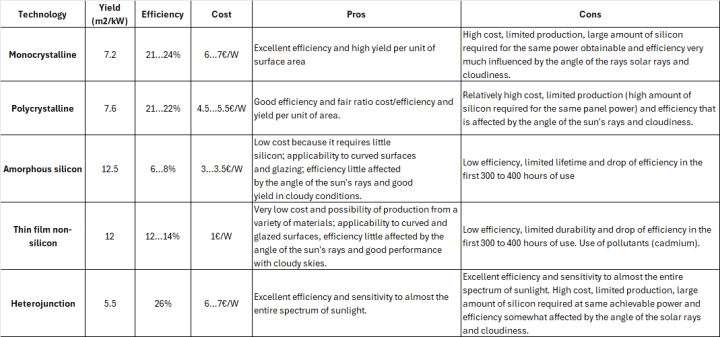
Below, we will describe the techniques in use for the construction of photovoltaic panels, summarizing the main features in Table 1.
Crystalline Panels
Modules based on crystalline silicon photovoltaic cells were the first to be produced on a large scale and are among the most efficient, especially when made with synthetic semiconductors such as gallium arsenide that’s reserved, however, for military and aerospace implementations.
Of the many materials that can be used in the construction of photovoltaic modules, silicon is currently the most widely used, since it is available in large quantities on our planet and is widely used by the electronics industry, which has seen strong development of refining, processing and doping methods in recent decades.
Waste from the processing of electronic components can be used in photovoltaic panels, since a lower level of purity is required for silicon. The first solar panels (the “first generation” ones) were the so-called “crystalline” ones, which are made by employing still current two technologies: monocrystalline semiconductor (c-Si) or polycrystalline.
The former is made by melting the semiconductor and growing it back onto a seed crystal that defines the orientation of the crystal structure itself. For the latter, a metallurgical process is used, which produces a disordered crystal structure in which the crystals are randomly oriented.
Monocrystalline silicon cells have a higher efficiency (today they reach as high as 25%) but cost more. Polycrystalline silicon cells are cheaper; however, they have lower efficiency (around 23%) because part of the electrons released by light remain imprisoned in the crystal structure and also because the different orientation of the crystals hinders the light somewhat.
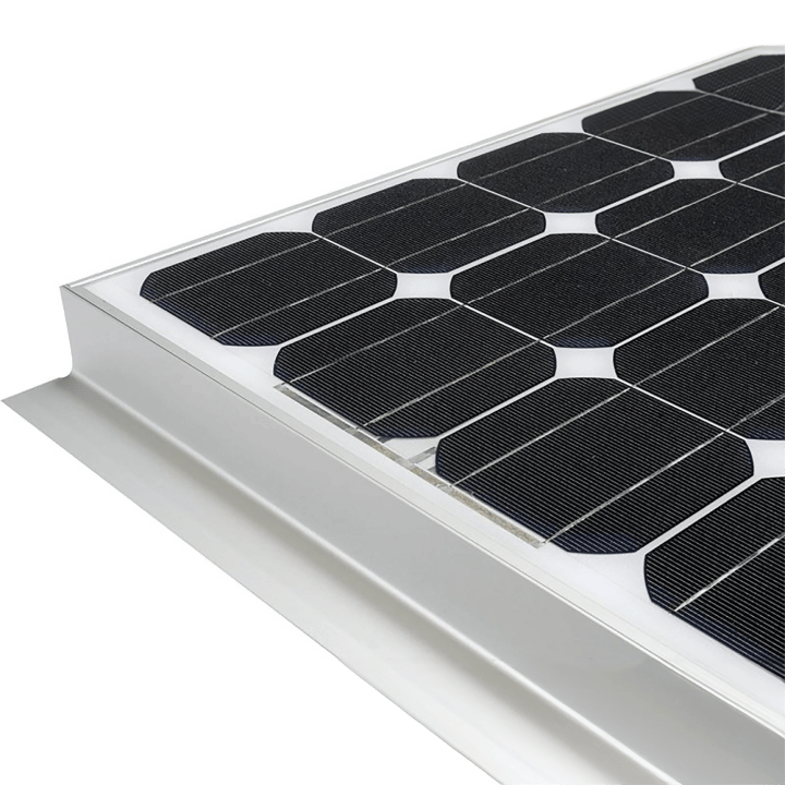
Crystalline photovoltaic panels are made by gluing several solar cells (typically 1.5 W each) onto a plate, as can be seen in Figure 1, and connecting them in series and parallel until voltages of 12 V, 24 V or higher are obtained. They are capable of delivering powers of even several hundred watts.
Knowing that the panels are used to charge batteries, one always makes sure that the voltage delivered is at least a few volts higher than that of the batteries themselves: typically 15 V or 28 V. Crystalline modules have two flaws: they cost a lot, and have good efficiency only if light reaches them in the optimal direction (when light strikes them perpendicular to their surface, with a deviation of ±20°).
This means that for much of the day their efficiency is poor. A crystalline panel inevitably sees its performance degrade over time, meaning that its efficiency is degraded by about 1% per year by exposure to the sun; on average, for a crystalline photovoltaic panel there is a 20% drop in 25 years.
Monocrystalline silicon has to be ultrapure and has high costs because its manufacturing process is very complex and requires temperatures as high as 1,500°C to melt the silicon and regrow it pure; therefore, to keep solar panel costs down, polycrystalline silicon is used, which is less performing but also less expensive, while still being able to guarantee a panel lifetime of 25 to 30 years.
The characteristic feature of polycrystalline silicon is that the crystals are still aggregated with each other, but with different shapes and orientations. Refinement of the polycrystalline silicon production process now makes it possible to make cells with electrical performance only slightly inferior to that obtainable with the monocrystalline process.
The most widely used type of photovoltaic panel is the “double-glass” type, consisting of two highly weatherproof transparent panes held together by plastic silicone. Between the two panes of glass are inserted silicon cells of various shapes (circular or square with rounded corners), about 0.3 to 0.5 mm thick and 25 to 100 mm in diameter.
To make the interconnections, the two faces of the silicon cell are metallized in some areas and the part exposed to the sun has the typical grid appearance, to allow as much light as possible to pass through. Small-power solar cells are constructed by diffusion (at 800°C) of pentavalent impurities (phosphor) onto a pure P-doped semiconductor substrate to form a junction at a depth of about 5 µ.
In this way, the semiconductor N layer is thin enough to allow light directed at the junction to pass through it. The substrate is electrically connected to the positive pole, while for the negative, the N area is metallized by making thin aluminum strips that converge on a single electrode.
The electrical connection between the photovoltaic cells is achieved through two metal contacts, one on the exposed face and the other on the opposite one, normally obtained by vacuum evaporation of metals with very low electrical resistance.
While the back metallization covers the entire face, the front metallization consists of metal strips that serve to draw current from the anode of each cell without obstructing the passage of light too much. The next step in the processing of a cell is the deposition of an anti-reflective layer no more than 1 µ thick, for which vacuum-evaporated titanium oxide is usually used.
Amorphous Silicon Panels
An alternative — but very viable — technology to the crystalline dates back more than 30 years and is that of amorphous silicon (a-Si). Cells of this type are composed of semiconductors in which atoms are chemically deposited in amorphous form (i.e., disorganized at the crystal lattice level) on the supporting surface.
The latter technology has the advantage that it requires minimal amounts of silicon (the thickness of the semiconductor is on the order of a micron, not surprisingly suitable for making thin-film modules); however, the resulting modules have a lower efficiency than that typical of crystalline technology.
The non-uniform orientation allows obtaining an average efficiency equal to that of the most valuable monocrystalline, since in the amorphous structure — atoms being oriented in various directions — solar radiation effectively hits a good number of atoms, whatever its direction of arrival.
As a result, in installations where the panels are fixed and when the sky is a bit cloudy, the adoption of amorphous systems guarantees a more uniform production of electricity throughout the day. In fact, with the crystalline as long as the sun is striking at the optimal angle (at noon...) the current produced is more than double that of an amorphous, but then it drops; on the other hand, the amorphous receives light more or less well from any direction, so it takes advantage of the sun throughout the day.
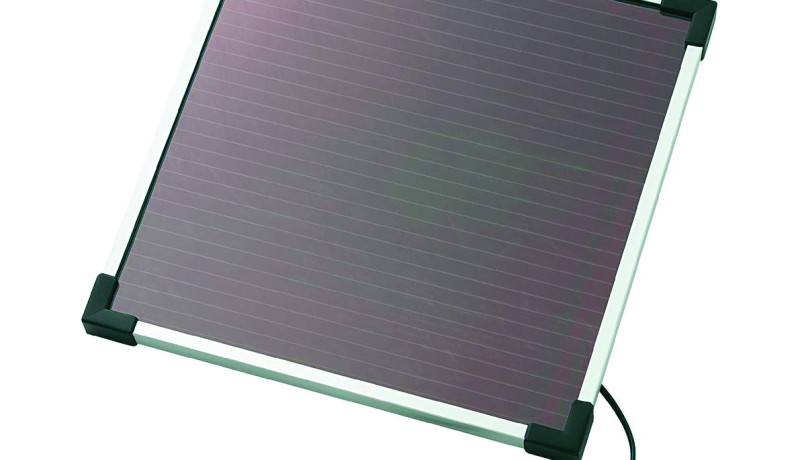
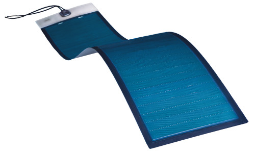
An example of an amorphous silicon photovoltaic panel is illustrated in Figure 2.
Thin Film Modules for Photovoltaic Systems
One of the latest manufacturing technologies that is set to radically change the way photovoltaic systems are conceived is thin-film, which includes components made of micro-spheric silicon, mounted on a flexible module, or amorphous silicon or synthetic semiconductors.
A common feature of all is the very thin thickness (hence the name) of the active layer. The modules made are only a few millimeters thick and consist of layers of semiconductor material that is not necessarily silicon, usually deposited as a gas mixture on low-cost substrates (glass, polymers, metals). Thin-film technology includes traditional amorphous silicon (a-Si) modules, which are currently the best-selling ones, but also tandem and triple-junction amorphous silicon panels.
The tandem technique dates back several decades and has also been adopted in crystalline panels; it is understood by considering that a certain semiconductor has a peak sensitivity at a certain wavelength of light.
To achieve maximum performance under different lighting conditions, taking full advantage of the spectrum of sunlight, one can combine cells composed of different semiconductor materials: for example, silicon (from the infrared to the middle of the visible spectrum) and gallium arsenide or other synthetic semiconductor with high extraction work, for the upper part of the visible range.
In this way, both direct sunlight (which has a lower color temperature and thus a longer wavelength) and reflected light from the sky, which is cooler and has a shorter wavelength. For example, a module built with this type of technique, compared to crystalline silicon has yes lower specific efficiency, but for the same power it manages to produce on an annual basis 20% more energy, since it has a better response to diffuse solar radiation (the light reflected from the sky). An example of a thin-film solar panel is shown in Figure 3.
An evolution of the tandem technology has been patented by Unisolar, and is known as Triple Junction. Instead of pairs, it employs triples of solar cells, each made of its own material.
As far as durability is concerned, the thin-film technique and in any case the amorphous silicon technique suffer from a less constant drop in yield. In addition to this, the thin-film technique has many advantages: besides being cheaper and allowing a more uniform yield throughout the day, it allows the construction of flexible types of photovoltaic modules for a multitude of uses, including to be bonded to curved substrates made of steel (sheet metal roofs) and other material (PVC sheathing, etc.).
The minimal thickness allows the modules to be applied not only to curved and flexible surfaces, but also to the glazing of buildings, while still allowing a fair amount of light to pass through. This explains why the thin-film technique is growing rapidly, and alongside the older solutions — namely, those just described — new technologies based on synthetic materials are being developed.
One of these employs a layer of cadmium telluride (CdTe) on top of one of microcrystalline cadmium sulfide (CdS), which have very low production costs because the technology used for the purpose does not require the achievement of the very high temperatures required by silicon melting and purification.
About cadmium telluride, it is an artificial semiconductor that makes it possible to make photovoltaic modules with peculiarities quite similar to those obtained from expensive gallium-arsenide. The mechanical characteristics are excellent: with an active layer of only 5 µ, it is possible to build cells with efficiencies of more than 13%. However, large-scale production is still difficult, and the problem of overall module efficiency remains to be solved.
As for microcrystalline cadmium sulfide, the construction technique is quite inexpensive: the material is applied to a metal substrate, spraying it like a paint. Unfortunately, the production of this kind of photovoltaic cell has some disadvantages: the toxicity of cadmium and the low yield that can be obtained. Furthermore, if the photovoltaic panel catches fire and reaches very high temperatures, there is a risk of cadmium being released into the air.
Gallium arsenide (GaAs) is also used in the fabrication of thin-film panels, which is capable of very high yields (40%) due to its better sensitivity to sunlight and higher extraction potential, resulting in a higher useful voltage per cell than that obtainable from silicon.
One reason why the performance of gallium arsenide is better than that of silicon to solar radiation lies in the fact that it is more sensitive to the highest energy component of the sun’s rays: the ultraviolet component. Considering its high cost, this semiconductor is mainly used for military or advanced scientific applications.
Two other synthetic materials intended for solar cell production are copper indium selenium (CIS) and copper indium gallium selenium CIGS, which are very complex and expensive from a constructional point of view.
Another technology that we can consider hybrid is the microspheric silicon technology: it employs polycrystalline silicon reduced to spheres about 0.75 mm in diameter, caged in an aluminum substrate. Note that of the technologies described, amorphous and microspheric allow the module to bend without damage. In the case of amorphous, it is because there is no crystalline structure of the material to prevent it from bending. And in the case of microspheric, it is not the cell (sphere) that bends, but the honeycomb grid on which it is arranged.
Thin-film panel efficiencies are typically 21% for crystalline silicon, 18% for organic materials (CIGS go up to 16%) and 14% for amorphous silicon. For more details, you can take a look at the Amorphous Silicon and Thin Film Technology text frame in this article.
Hybrid Technologies
In addition to those just listed, there are technologies for building solar panels that combine the basic technologies. The first one we analyze is HJT, or Hetero Junction Technology, which consists of exploiting PN junctions made up of different substances from each other; the cells are composed of a crystalline silicon layer as the support surface for one or more amorphous or crystalline layers, each of which is optimized for a specific band of wavelengths that make up sunlight (Figure 4).
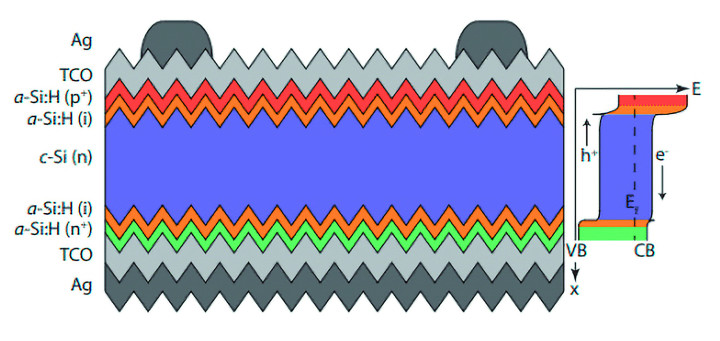
An example is Japanese Sanyo’s HIT (HIntrinsic Thin layer) technology: it is based on a thin monocrystalline silicon wafer surrounded by an ultrathin amorphous silicon film. These structures, while requiring advanced and expensive techniques, offer yields of up to 19% and last up to 30 years, outperforming conventional panels.
Panels made with hetero-junction are based on three materials: monocrystalline silicon, amorphous silicon and ITO (indium oxide thin film); with the most promising technique, an efficiency of 27% has been achieved.
Concentrated Photovoltaics
Although solar energy is more than sufficient for human needs, in practice it would be impossible to harness even half of it in conventional photovoltaic systems; this is because the annual production of refined silicon (i.e., suitable for use in electronics) is about 30,000 tons. Assuming reserving 50% of it for photovoltaic panel production and knowing that using the crystalline technique requires 20 kg of silicon per kWp to be produced, each year world production could increase by 750 MW (0.75 GW); considering that existing plants typically lose 1% efficiency each year, it is not true that the photovoltaic production can go up by 0.75 GW annually, since it actually loses some of what already exists.
For this reason, conversion efficiency needs to be raised. One way to do this is to use systems that can concentrate light without increasing the area of the solar cell, using converging lenses; this allows efficiencies of more than 40%. However, the technique has the drawback of requiring cooling of the cells, which, being invested by concentrated light, heat up more than conventional cells and, if not properly cooled, get damaged. However, the efficiency of this type of photovoltaic panel is limited by thermal agitation; otherwise, it would rise as high as 50%.
Next Steps
So far, we have reviewed the types of photovoltaic panel available on the market, with all their different features and capabilities. In the second part of this article series, we will see how to integrate them into the most common connection schemes with charge controllers, battery storage systems and inverters, both in off-line and grid-connected configurations. Meanwhile, don’t unplug us, please!
Amorphous Silicon and Thin Film Technology
Thin-film technology requires minimal amounts of semiconductor because it consists of very thin and, therefore, also very transparent structures. It has low production costs and, compared to crystalline technology, it allows panels to be made that are less fragile and more tolerant of the angle of exposure to light.
In particular, some thin-film modules are also walkable, flexible and adaptable to curved and glazed structures. The only flaws are low efficiency and stability over time. The low efficiency is compensated by the fact that the module is more uniformly sensitive to light than is the case with crystalline modules; in other words, the efficiency is about the same within a broad angle, which makes the modules very suitable for use in fixed installations and gives better efficiency against diffuse light, that is, when the sky is overcast.
Unlike crystalline technology, in which the semiconductor material is solid in wafer form, thin-film technologies involve the material being deposited by extracting it from a gas, which for amorphous silicon typically is silane (SiH4) or trichlorosilane (SiHCl3); these gases are then the same as those used for decades in the production of semiconductor electronic components by epitaxial growth.
Similar is the technology based on synthetic semiconductors such as CdS, CdTe, etc. The deposition of semiconductor from a gas that contains it, makes it possible to fabricate very thin layers (a few microns...) on a wide variety of substrate surfaces, using lower temperature processing (800 °C) than that required to fabricate the junctions of mono- and polycrystalline panels. However, since the processing of thin-film modules requires the use of materials with special characteristics (amorphous silicon, cadmium telluride, indium diselenide, and copper) there remain still to be resolved several technical issues, especially about the stability of electrical performance over lifetime.
Unlike crystalline modules, thin-film modules essentially consist of a large interconnected junction(s) obtained by deposition of a doped material of acceptors (rich in gaps) on a donor-doped one (rich in electrons); for example, cadmium sulfide on cadmium telluride, for CdTe/CdS synthesis technology.
The uniformity and the ability to make flexible modules make amorphous silicon a popular product for integration with architectural elements. Amorphous silicon was the first material used for the production of thin films. Unfortunately, the very nature of amorphous silicon, which does not have a defined molecular structure, severely limits the product's performance in terms of conversion efficiency, which remains well below that of crystalline (5 to 8% for the best amorphous multi-junction cells).
For thin film, a number of problems related to performance stability over time remain to be solved because nearly 10% of the manufacturer's claimed power performance is lost in the first 300 to 400 hours of exposure, although it then stabilizes more than crystalline, which uniformly loses about 1% per year.
One construction technology for solar panels that is gaining popularity is triple junction technology: in it, the photovoltaic module consists of a three-junction thin-film structure stacked on top of each other, each sensitive to a certain portion of the sunlight spectrum. The reduced thickness and thus transparency of the layers allows light to reach the innermost one.
Current thin-film cell technologies apply to both amorphous silicon and synthetic materials and are as follows:
- Amorphous silicon, in which silicon atoms are chemically deposited in an amorphous, i.e., structurally disorganized, form on the supporting surface, which can be glass, stainless steel or other metal,
- Cadmium Telluride (CdTe, N-semiconductor) and Cadmium Sulfide (CdS, P-semiconductor) deposited on a copper and carbon or titanium-based layer, which acts as a base and closed on top by tin oxide and glass,
- Gallium arsenide (GaAs),
- Copper indium gallium indium copper diselenide (CIGS); between two electrodes, formed by a steel foil that acts as a support and one of zinc oxide placed under the protective glass, there is a layer of cadmium sulfide (P semiconductor) and one of indium copper gallium diselenide (N semiconductor),
- Copper indium diselenide (CIS).
Editor’s notes: Interested in ESP32 and DIY projects? This project originally appeared in Elettronica IN.
Discussion (13 comments)