[Partner Content] The new PIC16F131xx family of microcontrollers offered by Microchip is a perfect response to the constant evolution and ever-advancing miniaturisation of electronic equipment. Their functionalities facilitate economical power management and designing controllers with predictable response times.
New family of Microchip systems with configurable logic blocks
The new PIC16F131xx family of microcontrollers offered by Microchip is a perfect response to the constant evolution and ever-advancing miniaturisation of electronic equipment. Their functionalities facilitate economical power management and designing controllers with predictable response times.
Ensuring time-predictable circuit behaviour is one of the key requirements for the designers of state-of-the-art embedded systems. In practice, it boils down to limiting the time of response to changes in the controlled processes, i.e. instant response to input data from sensors, communication ports or user interface. It can be ensured by increasing the system’s computational power, but this is in fact a suboptimal method, as it results in wasting large amounts of energy. In order to avoid program-based operation of basic processes, the Microchip microcontrollers utilise core independent peripherals (CIPs). The configurable logic block (CLP) is a new solution integrated in the new family of 8-bit microcontrollers offered by the manufacturer, i.e. PIC16F131xx systems.
Parameters and peripherals
This part of the text discusses the CIP and CLB solutions and the manner in which they make it possible to retain the system’s computational power to manage applications, while they fulfil simpler tasks (operation of buttons and certain displays, recalculating values obtained from converters). However, let us firstly take a closer look at the PIC16F131xx microcontroller specifications and design.
These systems are based on the classic 8-bit Harvard architecture. They come in through-hole (THT) and surface-mounted (SMD) packages. The DIP, DFN, SSOP, TSSOP, SOIC and VQFN packages are available with 6, 12 or 18 input/output pins. A wide range of acceptable supply voltages, i.e. from 1.8 V to 5.5 V DC, is a significant advantage, too. They are clocked with the 32 MHz frequency signal, and the minimum instruction execution time is 125 ns. The systems include from 256 bits to 1024 bits of SRAM operating memory and up to 14 kB of program memory (FLASH).
Designers are provided with an extensive selection of hardware peripherals, such as PWM signal generators, 8- and 16-bit counters/timers, an EUSART serial bus controller, MSSP (Host Synchronous Serial Port) module capable of operating in the I2C or SPI interface operation mode, configurable comparators with reduced response time (50 ns), an 8-bit digital-to-analogue (DAC) converter and a 10-bit analogue-to-digital converter with a module enabling computation (ADCC), i.e. hardware-based processing of the values obtained. Note also the CIPs included in the systems presented here.
Core Independent Peripherals
Microchip has been including CIPs (Core Independent Peripherals) in its products for some time now, both in the PIC® and AVR® product families. They facilitate performing certain tasks (e.g. communication with sensors) in the background, without using the CPU processing power, which thanks to that is entirely available for the main program execution, leading to reduced energy consumption and simplification of the program itself. Dedicated peripherals can be used for data transmission (I2C, CAN, USB), counting down the time (timers), PWM signal generation or handling analogue signals (ADC, OP-AMP, DAC).
CLB peripheral
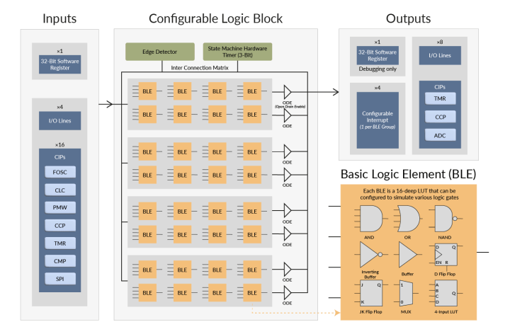
The key innovation introduced in PIC16F131xx controllers consists in providing their structure with independent, configurable logic elements (their operation principle results in the fact that this system is treated as a CIP peripheral). This technology is described as CLB (Configurable Logic Block). It ensures functional safety and instant response time. The CLB technology is based on structures used in FPGA systems, i.e. designs ensuring the shortest possible input signal processing times. CLB uses basic logic gates that can be freely configured by a designer for the purposes of a specific application. Additionally, it facilitates target device miniaturisation by excluding external components and reducing the PCB size. Precise determination of the task execution time is a key advantage of the CLB technology. It results from the fact that, even though these tasks involve relatively complex procedures, their execution is always based on hardware.
Available logic gate types
The CLB structure in PIC16F131xx microcontrollers includes discrete components creating 32 identical cells, each of which is a basic logic element (BLE). All of them are clocked with the CLBCLK signal leading edge. Depending on the actual needs, a cell simulates a single logic system defined during the programming stage. It can be:
AND gate (max. 4 inputs);
NAND gate (2 inputs);
OR gate (max. 4 inputs);
NOR gate (2 inputs);
XOR gate (max. 4 inputs);
XNOR gate (2 inputs);
NOT or buffer (1 input and output);
D or JK flip-flop;
configurable LUT (Lookup Table) – up to 4 inputs.
Moreover, you get an extensive input and output signal selection. The conditioning values may originate from a 32-bit register available on the program level, or they can represent the status in microcontroller I/O lines, or they can originate from the PWM generator, timer/counter or even the SPI serial bus buffer. The same is true for the configured gate leads which can be connected to a converter, timer or physical output lines (pins) of a system during the programming stage. Each of the four cell groups can optionally generate an interrupt handled by the program. Note also that the BLE cells come with tri-state outputs. Available CLB structure cell set-ups
To sum up: a designer obtains a fully configurable structure that is similar to FPGA and implemented in a state-of-the-art, 8-bit microcontroller. The 102 bytes of the internal memory are provided to store settings. Finally, there is also the question of setting up the unit.
Set-up and programming
Setting up FPGA systems is often considered to be an activity requiring specialist, in-depth expertise. However, the tools for handling PIC16F131xx products are developed in a manner that makes using them quite straightforward. Therefore, even beginner developers are able to quickly master the basics and achieve the intended results.
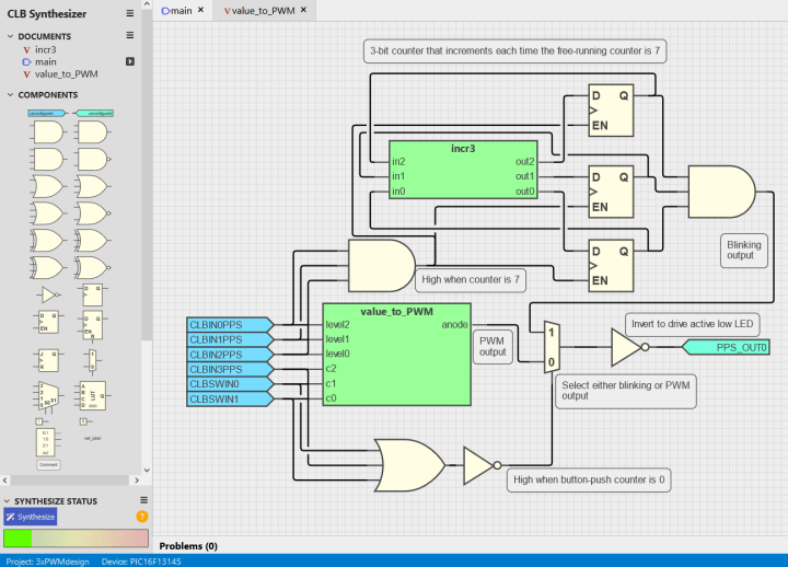
Firstly, a CLB is set up using the dedicated CLB Synthesizer software based on a graphic interface. Its use is equivalent to creating a block diagram, which makes the program quite clear, even if you are not familiar with all the functionalities of this environment.
The software is provided as a plug-in to the proprietary Microchip’s IDE, i.e. MPLAB® X. The tool can be used in a regular browser, as it is made available as a Web-based application. The CLB Synthesizer creates a set-up file which can later be imported to a design or a source file (.clb) written in the VERILOG language. Example set-up created using the CLB Synthesizer environment
The diagram is built by dragging blocks and connecting them between one another, with predefined input/output lines. The process of operating MPLAB® involves seven simple steps:
Setting up clocking signals.
Setting up digital blocks, such as UART, I2C, TMR, etc.
Adding analogue peripherals, such as ADCC and DAC.
Adding a CLB peripheral to a design by creating a block diagram with components included in BLE cells and defining connections between them and input signals.
Synthesis, i.e. creating a set-up file.
Finally, a function must be defined and assigned to microcontroller inputs/outputs used in the design.
The last step involves generating the Melody code.
Note also that, for educational purposes, Microchip has created a number of practical examples of CLB applications for various task performance. They include, among others:
handling a shift register for programmable (addressable) WS2812 LEDs;
hardware-based debouncing of button signals;
Manchester modulation encoding/decoding;
multiplexing a 4-bit value into signals controlling a 7-segment display;
frequency processing.
The video presented below shows one of such applications, i.e. creating a controller for 7-segment LED displays. Note here that this CLB set-up creates a program that operates totally independently from the microcontroller core. In practice, it could replace a dedicated controller system by simplifying and reducing the circuit of the designed device, and also by reducing its energy consumption.
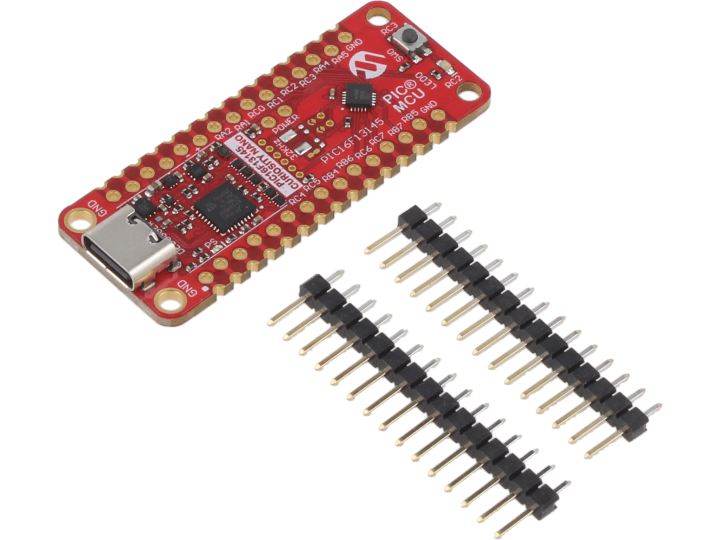
Curiosity Nano development kit
The Curiosity Nano platform has been created to provide Microchip customers with development kits presenting the capabilities of the latest microcontrollers marketed by the company. The development boards are designed in a convenient format, including an integrated debugger, programming device and access to microcontroller pins. It makes them perfect training and educational tools. Obviously, a dedicated Curiosity Nano has also been developed for the PIC16F131xx product family. The board can be connected to a prototyped circuit using pin connectors
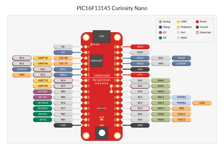
EV06M52A is a development kit equipped with the PIC16F13145 microcontroller. The circuit includes a USB-C port for power supply and programming. The LDO MIC5353 regulator supplies voltage to the microcontroller. Optionally, the circuit can be fitted with an RTC quartz-crystal resonator (32.768 kHz). The power supply and programming status is indicated by a green LED. A yellow LED connected to one of the microcontroller outputs can be operated by the microcontroller. The board also features a button. EV06M52A board component layout and description of leads.
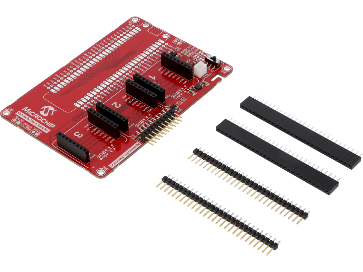
Adapters
Functions of the development kit can be extended by applying adapters dedicated to Curiosity Nano boards.
The above-mentioned products are equipped with universal (female) pin connectors to mount the Curiosity Nano board. As far as the AC164162 is concerned, the circuit comes with several interesting components, such as three connectors compatible with the mikroBUS™ standard used in the Click modules offered by Mikroe. Note also that the TME product catalogue includes more than one thousand of various models of these boards. The PCB also features the Xplained Pro extension connector. Moreover, the entire unit can be supplied by batteries, as the adapter comes with an integrated charging and power management system that is compatible with lithium-ion and lithium-polymer cells. AC164162 adapterText prepared by Transfer Multisort Elektronik Sp. z o.o. https://www.tme.eu/dk/en/news/about-product/page/60236/small-pic-microcontrollers-with-integrated-fpga-features/

Discussion (0 comments)