Sensor Testing with the ESP32-S3-Based Sensor Evaluation Board
on
Sensor Testing Simplified
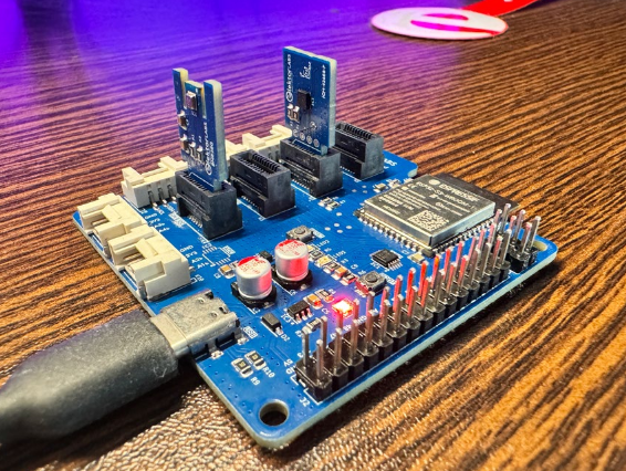
Before starting any project, we begin with an idea — a way to solve a problem or improve an existing solution. Then comes the planning stage, where we identify what’s needed to bring that idea to life: the tools, equipment, and components that will make the project a reality. For sensor-based projects, this can often mean repeatedly testing different sensors, swapping out hardware, and troubleshooting to get everything working just right. That’s where the Sensor Evaluation Board comes in (Figure 1).
The idea of modular edge cards for each of these commonly used sensors can be employed to tackle this issue. By simply plugging in an edge card dedicated to a specific sensor, one can now swap sensors effortlessly, with no wire clutter or reconfiguration required. This modular approach streamlines testing and keeps desk space optimized, allowing multiple sensor setups to be tested on the same board seamlessly. Integrated with high-precision external ADCs, the Sensor Evaluation Board transforms the process, saving time and ensuring that every setup can be tested with accuracy and ease. Whether one is involved in environmental monitoring, IoT applications, or simply experimenting with sensor data, this board offers a seamless and structured approach to transforming concepts into fully functional prototypes.
Design and Architecture
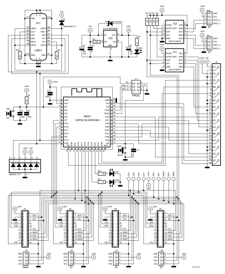
The schematic in Figure 2 outlines a design aimed at simplifying sensor testing with the ESP32-S3 module as the central controller. The ESP32-S3 was chosen for its dual-core capabilities and strong support for Wi-Fi and Bluetooth, making it suitable for IoT applications.
Compared to options like STM32, the ESP32 offers broader community support and simpler integration for Wi-Fi-focused projects. Moreover, integrating a ESP32 WROOM Module is much easier in your projects as compared to other microcontrollers as the WROOM modules already have the antenna front end designed along with other core components to use with the MCU, which further decreases the number of components to make your prototype work. You can address to Figure 3 which shows the PCB layout of the board.

The board includes two ADS1015 ADCs (IC1 and IC2) to address the limitations of the ESP32-S3’s internal ADCs. Both of them have four analog inputs (channels). The analog inputs of the first ADC are connected to 2.54-mm pitch header pins and the analog inputs of the second ADC to two Grove connectors (two channels each, together with VCC and GND). The ADS1015 provides reliable 12-bit resolution, which is adequate for most sensor tasks while remaining cost-effective. Although a higher-resolution ADC like the ADS1115 was considered, the ADS1015’s balance of performance (3300 Samples/s vs. 860 Samples/s) aligned better with the board’s purpose. However, one can use ADS1115 instead of the ADS1015 on the same PCB as both of these ICs share the same pinouts and footprint. As you can see, the ADDR pin of one ADC is connected to GND, the other one to VCC — which gives these chips different I2C addresses (more on this can be found in the datasheet).
For status indication, the board features two LEDs (LED1 and LED2) connected to GPIO14 and GPIO21 of the ESP32-S3. These LEDs can be configured for any application, such as displaying power status, communication activity, or custom debugging signals during sensor testing.
One I2C interface of the ESP32 (GPIO8 = SDA) and GPIO9 = SCL) is routed to the edge card receptables K1 to K4 and additionally to three Grove connectors K6 to K8 and one Qwiic connector K5. Similarly, the SPI communication interface is allocated as follows: SDI on GPIO11, SCK on GPIO12, and SDO on GPIO13. These lines are also connected to the edge card receptables; together with four CS (Chip Select) lines. This enables simultaneous use of SPI sensors across the edge card connectors without conflicts, enabling greater flexibility in sensor testing setups.
As said, the four edge card connectors (K1...K4) enable straightforward sensor swapping without any rewiring. These connectors are EC.8 edge card SMT connectors from ept , which are indeed quite robust for this application; they support up to 28-Gbps data transmission and a current capacity of 3.2 A (specs well above what is required here). However, their main advantage lies in their ease of use, allowing for seamless, frequent sensor module changes in a testing environment. Compared to traditional pin headers, these edge connectors make it significantly easier to streamline testing setups, with a claimed 500 insertion cycles that should hold up well over time.
Connector J1 is dedicated to programming the ESP32-S3 via UART, providing a straightforward interface for uploading firmware and making initial configurations. However, one can also flash firmware via the USB Type C Connection (K11) as well. J2, on the other hand, is a 2.54-mm header that grants access to the remaining GPIO pins of the ESP32-S3 and the first ADC (IC1). This additional access is valuable for connecting external modules or custom peripherals directly to the ESP32-S3, allowing flexibility for expanding the board’s functionality as needed during development and testing.
As stated before, the Chip Select (CS) line poses a unique challenge, as each sensor requires a dedicated CS pin when operating over SPI. To accommodate this, four separate CS lines are available on the edge card connectors, each with a unique GPIO assigned by the microcontroller. While this solution meets the needs of the current design, a multiplexing approach, or a GPIO expander could be considered for future versions to allow dynamic assignment of CS pins. For now, this configuration effectively supports simultaneous operation of multiple sensors, enabling flexible and straightforward sensor module swapping.
Modular Sensor Options
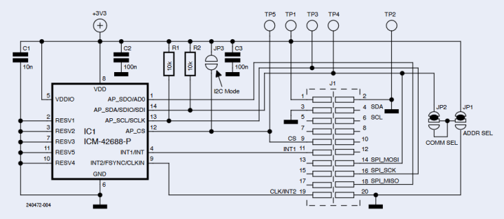
Two edge card sensor modules were created for the board: a BME280 environmental sensor and an ICM42688 IMU sensor. The schematic diagrams of these modules were based on their respective datasheets; however, for reference, you can see them in Figure 4 and Figure 5. Both edge cards share identical dimensions 23.55 × 13.55 mm (Figure 6), with standardized pinouts for I2C and SPI lines to maintain compatibility.

For testing these sensors, I utilized libraries that simplified the integration process. For the ICM42688, the ICM42688 library by finani was used, which proved to be user-friendly and included examples covering various functionalities such as I2C and SPI modes, interrupt handling, and more. For the BME280, I relied on the Adafruit_BME280_Libraryi> , which is well-known for its simplicity and ease of use.

When designing the edge card modules, I selected the 02x10 Connector odd/even symbol in the schematic and used the Samtec_HSEC8:Samtec_HSEC8-110-X-X-DV-BL_2x10_P0.8mm_Edge footprint from KiCAD’s default library for the PCB layout. For the edge card connectors on the Sensor Evaluation Board, I downloaded the footprint file directly from the manufacturer’s website and added it to my KiCAD library using the Library Loader program.
Regarding the physical specifications, the EC.8 connectors used on the board are designed to support 1.6-mm-thick PCBs. To ensure compatibility, I specified a 1.6-mm PCB thickness when ordering the edge card modules from the PCB manufacturer.

Testing and ADC Limitations of ESP32
During testing, I evaluated both of the onboard ADS1015 ADCs. Unfortunately, only a single ADS1015 IC was available with me at the time, so I tested it in both locations separately. Despite this limitation, both configurations performed identically under normal conditions. However, the ADC at IC1 showed slightly better noise performance. This is likely due to its position, being closer to its header pins and further from the board’s power section. That said, this noise difference is negligible for practical purposes.

When comparing these external ADCs to the ESP32-S3’s built-in ADC, the improvement is stark. The ADS1015 offers far better accuracy and significantly reduced noise, even with the ESP32-S3 clocked at 20 MHz. The difference in performance is almost incomparable — truly a “day and night” contrast — making these external ADCs a worthwhile addition.
Beyond the ADC testing, this board’s modular design truly shone when swapping and testing the edge card sensor modules. While I currently have only two modules — the BME280 and ICM42688 — the flexibility, they provide has inspired me to expand the collection. As shown in Figure 7, the compact size of the board, measuring just 64.7 × 66.6 mm, is another advantage. It’s smaller than the mouse sitting next to it in Figure 8, making it a perfect desk-friendly tool. This modular approach has proven incredibly useful for testing sensors and has earned a permanent spot on my workbench.

keyboard and mouse, demonstrating its desk-friendly dimensions.
Closing Thoughts: Modular Sensor Testing
Like any project, there’s always room for improvement, and reflecting on this design has given me several ideas for the next iteration. One area for refinement is the layout of the edge card connectors. While the present arrangement works, I encountered some difficulty soldering them using a rework station due to the tight spacing (Figure 9). This led me to use a hot plate method instead, just for these connectors. In future designs, I plan to space the connectors more generously to ensure better accessibility for soldering on both sides.

connectors, highlighting potential for future improvements
Another improvement would be relocating the bottom ADC (IC2) slightly further from the power section of the board. While the noise difference observed during testing was very minimal, optimizing its placement could further enhance signal integrity. At the time of designing, I speculated this might have a very minor impact, and testing confirmed that even small adjustments in layout can make a measurable difference.
Additionally, I would explore incorporating a multiplexer for the Chip Select (CS) lines on the edge card connectors. This would allow dynamic assignment of CS pins, making the design more scalable and reducing the reliance on predefined GPIOs for each edge card. It would streamline the integration of multiple edge cards and enable more flexibility in future designs.
Lastly, I’d consider adding an onboard OLED display for real-time feedback during testing. Features like displaying the sensor status or ADC readings directly on the board could enhance its usability and speed up debugging.
Overall, this project has been a valuable experiment in modular design and has proven its utility during sensor testing. While there’s always room for improvement, this version serves its purpose well and provides a strong foundation for future enhancements. With a few adjustments, I’m confident this board can evolve into an even more powerful and adaptive tool for embedded development.

Questions About Sensor Testing?
If you have questions about this article or sensor testing, feel free to email the author at saad.imtiaz@elektor.com or the Elektor editorial team at editor@elektor.com.
Editor's Note: The original article, "A Modular Approach to Sensor Testing" (240472-01), appears in Elektor March/April 2025.


Discussion (2 comments)