
Using EMI Shielding to Achieve Electromagnetic Compatibility Compliance
on
Technological advances, including the expanding rollout of 5G and the increasing reach of the Internet of Things (IoT), are leading to a greater need for electromagnetic interference (EMI) shielding. Achieving electromagnetic compatibility (EMC) compliance and reducing sources of EMI early in the design process are crucial to eliminating inefficiency, avoiding costly redesign, and preventing delays in product launch. Each design part or sub-system — from the enclosure to the module to the printed circuit board (PCB) — may incorporate EMI shielding.
A wide range of shielding options are available to engineers for every stage of the design process in almost every application, from commercial to energy infrastructure, defence to automotive. This article aims to give engineers some insight into what technological advances challenge current approaches to EMI shielding and to provide an overview of the materials on the market.
Electromagnetic Interference Is Everywhere
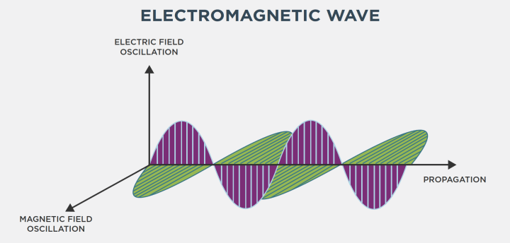
Electromagnetic fields are a feature of virtually every circuit. Oscillatory electric fields and magnetic flux lines (Figure 1) occur around the conducting path when an alternating current flows along a wire or through a PCB track. These become unwanted noise or interference when these fields become induced or transferred to another circuit or wire. This unwanted noise, generally referred to as EMI, can interfere with or disrupt the other circuit’s operation.An electrostatic discharge (ESD) is another form of EMI. ESD tends to be of varying frequency, whereas EMI typically occurs constantly. Any high-voltage, short-duration (high dV/dt) transients can cause erratic operation or permanent damage to sensitive electronic systems. Most electronic systems generate EMI unintentionally, including clocks, high-speed digital switching, DC/DC converters, and wireless interfaces.
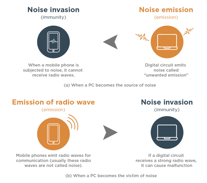
EMI emissions find their way into other circuits through either conduction or radiation. For example, small signal clocks passing along a PCB trace may radiate, typically above 10 MHz, since the tracks become effective antennas. The guiding principle behind EMC is that a circuit or system is immune to EMI (Figure 2).
Market Dynamics and Trends
Always-on connectivity has become ubiquitous. Whether at home, on the move, work, or in our car, our society never had so many benefits of reliable and resilient communications infrastructure. The rise of the IoT and its counterpart the Industrial Internet of Things (IIoT) and the growth of cellular communications have driven our need and dependence on wireless communications, which, unfortunately, is an essential enabler and a potential EMI source. The deployment of 5G wireless infrastructures, using previously unused, ultra-high frequency wireless spectrum, further expands the possibility of EMI. Consequently, ensuring products have EMI immunity has never been more critical.Electromagnetic Compatibility Standards
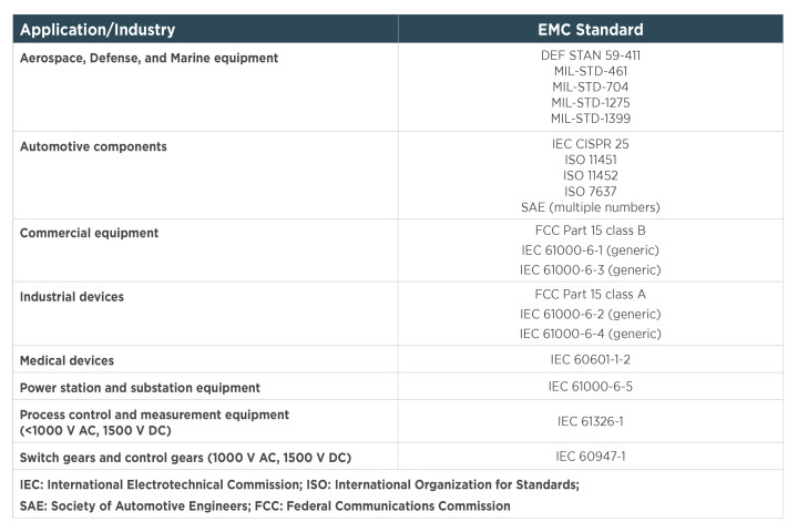
National and regional EMC standards, which typically align with internationally recognised EMC standards (Figure 3), provide manufacturers with specifications products must meet before sales occur. The standards stipulate the maximum emissions permitted from a product development and its immunity or susceptibility to radiated or conducted emissions. When embarking on a new design, it is recommended that design engineers consider the possibility of EMI and incorporate EMC countermeasures during the prototyping process rather than as an afterthought. An understanding of the EMI and EMC standards that apply, the likely sources of emissions, and circuit functions that may be more susceptible to EMI noise are paramount (see Table 1).
(Source: Kemtron Ltd, now part of TE Connectivity)
Achieving EMC Certification
Although an accredited EMC test facility can only perform EMC certification, there is a lot the engineering team can investigate before handing over the product to the test lab. Basic radiated and conducted emission measurements using a spectrum analyser or an EMI receiver equipped with suitable H and E field probes will indicate whether further testing or EMI countermeasures are required. These are expensive items of test equipment for a small product design team to acquire, but specialist EMI test and measurement rental companies offer a cost-effective alternative. Undertaking pre-compliance testing is highly recommended since it allows the design team to locate potential noise sources and implement EMI reduction methods such as shielding, ground planes, and decoupling. Exposing a product to EMI emissions is also important.Levels of EMI Shielding
Reducing EMI and making circuit functions immune to EMI require a systematic approach through the product design process. This includes aspects of the PCB design, incorporating ground planes and separating EMI noisy devices from sensitive analogue signal chains. Shielding components, functional parts, and modules offer a practical approach for many applications based on a three-level method, focused on enclosure, module, and PCB (Figure 4).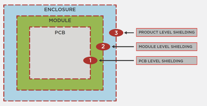
EMI Shielding Materials
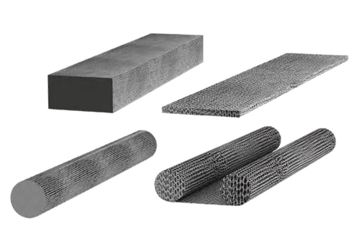
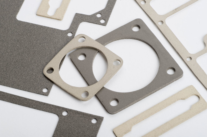
Examples of EMI shielding components include knitted wire mesh gaskets, electrically conductive elastomers, conductive fabrics, and metal fingers. Each type exhibits slightly different EMI attenuation characteristics and suits specific use cases. Figure 5 illustrates the attenuation performance of these four shielding types against frequency.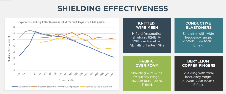
Discussion (0 comments)