

2A Maximum Power Point Charger [130145-I]
Here is an article proposal that I feel would fit nicely in the summer issue, or perhaps before summer, as a solar panel charger is best used during the summer. The design has been tested as a prototype in our boat last summer and is now rolled into a more permanent design that I will install, come spring.
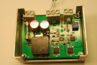
Here is an article proposal that I feel would fit nicely in the summer issue, or perhaps before summer, as a solar panel charger is best used during the summer. The design has been tested as a prototype in our boat last summer and is now rolled into a more permanent design that I will install, come spring. I even have spare PCBs in case you want to use as starting point in your lab :) The charger occupies just 70x60x27mm and is a tree-stage charger that can accept input voltages up to 32V and charge a battery up to 2A. It fast-charges at 2A max with a CC/CV characteristics up to 14.4V, then switches to 13.5V float charge. It also adjusts the float charge voltage, based on battery temperature.
Discussion (4 comments)

AndersG 2 years ago
The charge-profile for LiFePO4 is different, but quite simple. Basically you charge CC at 2A until the current drops under 2A, then CV until end. The float voltage must be selected sensibly to ensure a long battery life. I have settled on 13.6V (3.4V per cell) when the boat is not used for prolonged times and 13.7V when in use.
The values for R9, R10, R17, R11 are changed and the diode, D5 is removed. Connect a switch between 3 and 2 on the "NTC" connector to select between 13,6 och 13,7V
The values for R9, R10, R17, R11 are changed and the diode, D5 is removed. Connect a switch between 3 and 2 on the "NTC" connector to select between 13,6 och 13,7V
Reply
Show more
0 Comment(s)

TonGiesberts 11 years ago
We’ve designed a PCB that follows the design of the author very closely. The biggest difference of this design compared to the Demo Circuit 1568A from Linear Technology is probably the size of the inductor used (L1). Current rating is much higher than needed (11 A) but it has a very low DC resistance and consequently a low copper los. The highest output current the LT3652 can handle is 2 A. Question is of course what about core losses? With a fixed switching frequency of 1 MHHz these are higher with a larger core. But efficiency measurements gave satisfactory results. We used a solar panel simulator to test the circuit. There are many ways to do this. Simplest one is a big current source driving a large number of power diodes connected in series. The voltage across the diodes behaves very much like a real solar panel. We used a more intelligent and compact circuit where a number of 1N4148 diodes are placed in series and the voltage across is amplified to make a series regulator to reduce the dissipated power at no-load condition. Usually the datasheet of a solar panel specifies the open circuit voltage, shot circuit current and the maximum power point voltage and current at 1000W/m2 irradiation level. This last voltage can be set by P1. What the manufacturer of the LT3652 calls power tracking is in fact a regulation of the output power of the charger to maintain the set input voltage at (too) high loads. Or to put it in another way, the output current is reduced if the solar panel is not able to deliver the necessary power. If the output power is less than the solar panel can deliver the input voltage rises above the set maximum power point level. What we ask ourselves: is this really power tracking. What happens to the maximum power point voltage of the panel if the irradiation is much lower (or higher) than the level specified in the datasheet?
We also tested the circuit with a power supply. At a continuous 2 A output current the circuit and even the whole PCB gets hot. The effective on-resistance of the switch transistor in the LT3652 is 0.175 Ω which causes a larg part of the power loss of the circuit. To make sure the integrated circuit has enough cooling it has an exposed pad. Via’s in the pad on the PCB conduct the increase in heat to the copper plane on the bottom side. Here a larger opening in the solder mask makes it possible to add extra cooling. One way is to place a little aluminum bar between PCB and the aluminum case. The case then acts as an additional heatsink for IC1. Without it we measured the temperature of IC1 and it came close to 75 °C, the PCB just lying on our table at normal room temperature. The junction of IC1 will be even higher. If the PCB is placed inside a case at higher surrounding temperatures more cooling is a must. The aluminum bar can be 5 by 10 mm. The thickness depends on the protruding through hole components at the bottom side. Keep these lead ends as short as possible and make sure the little aluminum bar doesn’t make a short circuit to connections alongside of it (especially the solder pad of TP2) and the through hole components don’t make contact with the aluminum case. Use thermal glue to fix the little bar to the PCB or thermal compound between it and the PCB and glue in the corners.
The demo manual dc1568afa.pdf gives an overview of how to test the circuit. A good way to simulate a battery is given here, simply a large power resistor (or several in parallel, we used four 10 W resistors of 27 Ω) and a power supply.
Some measurements (a simple 22 kΩ resistor for the NTC)
Efficiency:
Vin[V] Iin[A] Vout[V] Iout[A] Pin[W] Pout[W] h
16 1.004 9.8 1.466 16.064 14.469 90.07
16 1.004 10.77 1.35 16.064 14.54 90.51
16 1.002 11.60 1.25 16.032 14.5 90.44
16.97 0.903 13.95 1.00 15.323 13.95 91.03
18.3 0.64 13.97 0.75 11.712 10.478 89.46
18.95 0.4 13.99 0.473 7.58 6.617 87.30
Other measurements:
No jumper (JP1):
charging stops at 14 V (14.35 PCB hot)
charging starts again when voltage drops to 13.9 V
after switch-on and just resistors at output: 2 V at output (0.3 A) until voltage rises to 9.5 V (at 9 V 0.28 A) then voltage and current rise to 9.8 V and 1.44 A.
with jumper JP1
charging stops at 14.2 V (14.56 if PCB hot)
charging starts again when voltage drops to 13.9 V
after switch-on and just resistors at output: 2 V at output (0.3 A) until voltage rises to 9.7 V (at 8.6 V 0.28 A) then voltage and current rise to 9.88 V at 1.43 A.
Bill of Materials 2A maximum power point charger (130145-1)
Resistor
R1 = 100 kΩ, 5 %, 125 mW, SMD 0805
R2,R5,R6 = 10 kΩ, 5 %, 125 mW, SMD 0805
R3 = 470 kΩ, 1 %, 100 mW, SMD 0805
R4,R10,R11 = 68k1, 1 %, 125 mW, SMD 0805
R7 = 1 MΩ, 5 %, 125 mW, SMD 0805
R8 = 499 kΩ, 1 %, 125 mW, SMD 0805
R9,R12 = 196 kΩ, 1 %, 125 mW, SMD 0805
R13 = 0Ω05, 1 %, 1 W, SMD 1206
P1 = 47 kΩ, 20 %, 0.15 W, trimmer, top adjust
Capacitor
C1 = 10 µF, 50 V, +80/-20%, SMD 1210, Y5V
C2 = 4µ7, 25 V, 10 %, SMD 1210, X7R
C3 = 2u2, 25 V, 10 %, SMD 0603, X5R
C4 = 10 µF, 25 V, 10 %, SMD 1206, X5R
C5 = 47 µF, 25V, 20 %, SMD 2220, X7R
C6 = 100 µF, 25 V, 20 %, Radial Can SMD
Inductor/Filters
FIL1,FIL4 = NFM41PC204F1H3L (Murata)
FIL2,FIL3 = NFR21GD4702202L (Murata)
L1 = 22 µH, 11 A, 20 %, 14.6 mΩ (Würth Elektronik 74435572200)
Semiconductor
D1,D8 = VS-50WQ04FNPBF, SMD D-PAK
D2 = BZX84-B10,215, SMD SOT-23
D3 = LED Red, 3 mm through hole
D4 = LED Green, 3 mm, through hole
D5,D6 = 1N4148, SMD SOD-123F
D7 = BZX84-B6V2, SMD SOT-23
T1 = SI4401DY-T1-E3, SMD SO-8
IC1 = LT3652EMSE#PBF, SMD 12MSOP
Other
JP1 = 2-way pinheader SIL, pitch 2.54 mm
JP1 = jumper 2.54 mm
K1 = PCB terminal block, 3way, pitch 5 mm
K2,K3 = PCB terminal block, 2way, pitch 5 mm
F1 = Fuse holder, 20x5 mm
F1 = Fuse holder cover
F1 = Fuse, antisurge, 2 A, 5 x 20 mm
TP1,TP2 = 1-way pinheader
Misc.
Case Aluminum, 57.5 x 72 x 28 mm, Teko 2/A.1
PCB 130145-1 v1.1
Reply
AndersG 11 years ago
Great work! A few comments:
Inductor: You are right about the tradeoff between resistive and core losses, nevertheless the figures for efficiency are OK compared with the ones in the datasheet and taking into account that it is a non-synchronous converter.
Heat: Yes, it needs cooling. In my prototype the PCB is mounted on standoffs with an aluminium slab underneath and silicone grease to help transfer. That cooling seemed to be OK even when pushed to the full 2A in laboratory conditions.
Tracking: The MP of a given panel is fairly constant with lightning and varies only slightly with temperature. Thus it is fair to say that the regulator will "track" the panel, by adjusting the load to keep the panel at the maximum power point. It will not however "track" if you substitute a panel with a different MP.
The whole idea behind this controller was to have a small and relatively inexpensive regulator so that you could equip each panel with a dedicated regulator, instead of feeding several panels to one big regulator. The latter might make sense in a fixed installation, but the former is preferable on a boat, where partial shading of panels is a problem.
Did you post the file dc1568afa.pdf here??
PS. It would be fun to do EMC on the circuit My first prototype was quite noisy and blocked the entire FM-band. The one I have now with screening and filters on the outputs is undetectable on the FM band.
Reply
Show more
4 Attachment(s)
1 Comment(s)

JohnHusband 11 years ago
I have recently had an idea that could be intergrated into the above design but am not so experienced at implementation. The idea is to use a commercially available satellite dish rotator arm, and a 60cm satellite dish (icecrypt includes fixings) suitably modified to allow elevation/declination to be controlled by a geared servo motor. The satellite rotator arm is controlled by DiSeqC cotrol protocol which would have to be simulated so as to track the sun by using energy harvesting technology. The solar panel is mounted on the dish. This model can be extended to create a much larger and more useful installation by a suitably talented electro-mechanical engineer. I think several small installations could be strung together to increase efficiency and provide a lot more fun for engineers.
Reply
Show more
0 Comment(s)
Updates from the author
AndersG 1 year ago
I have attached the complete schematic with the mods.