555 Class D Power Amplifier [130144-I]

With this project, I like to build a small class D amplifier based on a 555 timer IC. I also like to use only “common” components, so this project has great educational value and is easy to build.My goal is to produce about 5W RMS power into 4ohm. Distortion level should be less than 1%.Circuit description VERSION1 (see circuit diagram below)
With this project, I like to build a small class D amplifier based on a 555 timer IC. I also like to use only “common” components, so this project has great educational value and is easy to build.
My goal is to produce about 5W RMS power into 4ohm. Distortion level should be less than 1%.
Circuit description VERSION1 (see circuit diagram below)
In order to build a class D amplifier, we must convert the analog signal to a digital signal. In fact we like to use a pulse with modulated signal that follows the analog audio signal. This way, we can switch 2 power MOSFETs on and off in a very efficient way.
I use the NE555 as the heart of the PWM encoder. At the input, we have a standard NPN transistor input (Q4) biased by R10 and R9. C1 blocks all DC at the input. The idea is to modulate the way the charging capacitor C3 is loading with the analog audio signal.
In most standard 555 timing configurations, the timing capacitor is charged with a constant voltage, resulting in severe non linearities, especially at high output levels. To improve linearity, I charge the timing capacitor with the constant current. Therefore I use a current source at the input (Q3, R2 and R7) and a voltage to current convertor in the feedback loop of the 555. (Q1, Q2, R1 and R3) This way we get a real triangle wave on C3. (see image below “signal on C3 no signal.jpg”)
Oscillation frequency of the 555 is around 300 kHz.
Output signal is 0V – 18V PWM signal that switches on and off M1 and M2.
D1, D2, R4 and R5 are dealing with “on” and “off” timings and avoid that M1 and M2 are “on” at the same time (and avoiding to short circuit the power supply). R12, R14 and Q5 form a feedback circuit that improves linearity and distortion levels even more. L1 and C4 is a LPF around 25 kHz, removing all high frequency switching components.
I use a SMPS laptop power supply of 18V to test with (cheap). Initially I had switching noise in the speaker. Therefore I add a coil of 100µH to filter this out. Working fine!
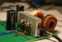
I built this circuit on a standard testing board, and I’m quite happy with the result. Audio sound “direct” and “clear” to me, with tight basses! I get about 6 W RMS power, what is fine for my first attempt J I do not have any distortion measurement equipment, so I’m not sure if my goal of <1% is reached.
About efficiency, the heat sink is cool at all levels, so this should be fine.
I attached some images and of course the schematic and also some scope prints of the output square wave and charging capacitor wave. I have also added a short video of the amp @ work. Don’t bother the bad sound quality of the movie; it’s the poor mic quality of my camera J
Possible improvements (VERSION2 tbc)
- Power MOSFETs must be controlled with 18V to be fully saturated (and “on”), if I raise the supply voltage on the MOSFETs and control with 18V from 555, MOSFETs are running hot as they don’t fully switch on. A voltage level shifter circuit is recommended here.
- I will to do some tests with IR2110 IC to achieve this, maybe there's a discrete solution? Maybe with a "charge pump"?
- Now we use “half bridge” 2 MOSFET configuration, therefore needing a big output capacitor, I did some tests with full bridge configuration (4 MOSFETs) in SPICE but I get a lot of cross over distortion. Need more investigation on this….
Any help, suggestions, or hints are welcome to improve this project!
Discussion (23 comments)
Bobbylebob 11 years ago
Hi frederik
I've just had a look to your circuit description. You are talking about efficiency matter and you're right when you say that a strongest drive give shortest rise and fall times and reduces loss.
You tried to increase to 18V but you've reached the maximum voltage, that's a good idea. However, you have to consider MOSFET's gates as small capacitors to properly drive them. When a transition from low to high occurs, the capacitor is at 0V and is charged through the 220R resistor. The peak current is then 18/220 = 82mA.This current is easily supplied by NE555's output but is well too low to give a fast transition
During High to low transitions, 220R resistors are bypassed by the diodes and the current is then only limited by NE555, and is probably greater than it can handle safely...
I guess that it also explains your interrogation about the assymetric waveform you found
Usually, it's recommanded to add MOSFETS drivers which can handle bigger currents (many amps !)
I suggest you to add a 18/0.2 = 100 ohms resistor in series with the diode to limit the falling current to the maximum allowable of 200mA.
You could also try to reduce the 220R to something like 150 or 120 which could speed up commutation, but pay attention to cross conduction...
Regards,
.David.
NuttyProf 11 years ago
Hi Frederick
I had a bit of thought. I have added a simple extra pair on the end to produce a bridge output in order to give extra power. This is purely a theoretical concept and has not been tested but I see no reason for it not to work. If the duty cycle is exactly 50/50 then in theory there will be no voltage across the Speaker A and Speaker B terminals.
The original had lousy FETS in the positive side (IRF9530 I think) with a high on resistance. Using the IRF4905 means a lower on resistance and better efficiency for the high side of the totem pole. The 555 only has to drive the one pair and the output of this pair drives the second pair. In my sketch I have left out the protection diodes across the FETs to the supply and also left out the full filtering circuit that goes on the output of the FETs before the speakers.
I would be keen to see if anyone takes up this idea. It should lead to a very efficient compact 25 watt RMS sine wave into 4 ohm output if my calculations are correct. Or 2 such amps (stereo pair) running from the PC PSU to power a pair of decent sized speaker boxes from the PC (maybe have to get a larger PC PSU to get the extra amperage for the amps). Maybe even design it to go into a 5 & ¼ or 3&1/2 rack drive straight into the PC. Or even 2 such amps (stereo) and a 12v to 19v supply all in one small box to use with a notebook PC on the 12 volts of a cars battery on summer camping trips. Here in South Africa this would be great for a party pack when the power goes out at a party.
Anyway the idea is there for anyone to take up. Please keep me informed should there be any takers.
Regards Harry Bartelink
frederik 11 years ago
TonGiesberts 11 years ago
Top copper and bottom copper of PCB 130144-1 v2.0 (72kb)
Plots of measurements of PCB 130144-1 v2.0 (28kb)
130144-1-555-class-d-power-amplifier-schematic-v200-1.jpg (1459kb)
130144-1v20-001.jpg (2018kb)
130144-1v20-004.jpg (1669kb)
130144-1v20-005.jpg (1373kb)
frederik 11 years ago
TonGiesberts 11 years ago
Here’s our first schematic and PCB design. Now that the design from Frederik is finalized we’ve decided to design a PCB and made some changes in component choices we think will improve the design. The PCB design is a bit more compact (131.22 x 99.47 mm). Components we think could be improved on are the electrolytic capacitors for power supply decoupling (C11/C25/C29) and the output signals (C14/C28). Also the capacitors for the pulse width modulation (C2/C16) are high quality polystyrene versions (radial types). The footprint also provides a double pitch for the use of silver mica types. The dielectric is critical for the linearity of the modulation. As an output inductor a bobbin type from Murata Power Solutions is used that (hopefully) has a more constant inductance versus current than the types from Pulse in the original design, thus less distortion in the output filter. This is also the reason it is a bit overrated (8.5 A). The footprint also has a double pitch for the larger 100 µH version. Should anyone one want to change the electrolytic capacitors in the output, the footprint has a double pitch of 5 and 7.5 mm. The capacitors in the LC-filter in the output (C12,C26) are polypropylene capacitors which are better suitable for this high current and high frequency application. To make measuring of the PWM signal from the 555 more easily we added two test points (TP1 and TP2). After filtering this signal first the distortion of the modulator can be measured and compare it to the total distortion at the output. That’s it for now and we’ll get back when we’ve had some first test results with our version.
PCB design from the lab for a first prototype (106kb)
frederik 11 years ago
some images of the final result!
dsc01321.JPG (635kb)
dsc01322.JPG (305kb)
dsc01323.JPG (432kb)
dsc01325.JPG (293kb)
frederik 11 years ago
I did some more tests on the frequency response.
With the 100µH + 680hF output filter I get a -3db point ant 15kHz at 8ohm load.
I changed the output filter inductor to 47uH, what corrects the problem.
Also I solved the problem of the 'speaker pop' when the relay is switching on. (due to the output capacitors storing DC) I add resistor of 15ohm to the 'off' side to the relay, solved.
I will finalise this project by building this amp in a metal case. I will use it in my living room now. Pictures will follow soon.
Frederik
frederik 11 years ago
I did some more tests and measurements to define output power and efficiency.
Please shoot if i make any mistakes :-)
1. POWER
I connected 4ohm 50W resistor to output and adjusted input signal to maximum output without visual clipping on scope. I got 15V peak to peak sinus on output, input signal is 1.6V peak to peak.
To calculate power:
P = U*I = (U*U)/R = (7.5V * 7.5V) / 4 = 14.06W peak
P rms = 0.707 * 14.06 = 9.94W rms
2. EFFICIENCY
I connected a current multimeter in the power supply line.
I disconnect input signal and short circuit inputs to ground.
Both speakers are connected; I measure 140mA current.
power use without any signal = 24V * 0.140A = 3.36W (good I think!)
I connect L and R 1kHz signal and adjust to max power output without viisible distortion. I measure 980mA
power use with L and R signal to full power = 24V * 0.980A = 23.52W
Efficiency = ((Prms left + Prms right) / P powersupply ) * 100
= ((9.94W + 9.94W) / 23.52W) * 100 = 84.52%
If my calculations are correct, Im a happy man!
frederik 11 years ago
TonGiesberts 11 years ago
frederik 11 years ago
I built a stereo version of the and i must say i'm impressed of the sound quality! I like amp without any feedback circuits, it's sounds very direct and tight....
I don't use the 555 buffer any longer, beause I had the same timing problem as mentioned before. I changed it to BD139/BD140 totempole buffer. This is working fine on the PCB.
About the PCB, I made some small improvements, some hole were not right sized, I forgot one track. Fixed now.
I think my goal is reached: Class D amplifier based on a NE555 and only basic common components used. I'm happy all other semiconductors are discrete! :-) I'm planning to build this amp for living room use.
Right now I use the CMOS version of the 555 (ICL555) what gives a more clean square wave. I don't hear any difference with the NE555,I think we can use this one anyway.
Possible improvements: relais output; when the output switches on, I get a 'plop' in the speaker, maybe the output resistors (2K7) should be smaller?
When I adjust potmeter so I get 50% duty cycle, I get a small oscillation around 15kHz. As soon I change dury cycle to 55% problem is solved.... Not shure how I can fix this, maybe the Elektor engineers know hw to sort this? :-)
Please feel free to post your reactions!
I have add pictures, schematic, pcb and a small movie of the amp at work!
dsc00559.JPG (520kb)
dsc00561.JPG (432kb)
555d V4 - Schematic and pcb.zip (150kb)
movie version4.zip (3870kb)
frederik 11 years ago
555d V3 sch.zip (96kb)
frederik 11 years ago
555d V3 sch.zip (96kb)
frederik 11 years ago
130144 schematics and pcb designspark.zip (125kb)
frederik 11 years ago
JD 11 years ago
frederik 11 years ago
Hi,
I made some small modifications; the current source around T2 is changed now. This should be more temparature stable.
I also add a speaker protection, speaker turn on 2 secs after power on and switches off directly after power off.
I'm planning to draw a pcb of a stereo version with protection on it.
Schematic attached!
Any suggestions, feel free to reply !
Frederik
555d V2 - Schematic.pdf (89kb)
frederik 11 years ago
Attached you'll find the new version, this time again with the extra 555 as buffer.
I increased the timing c to 330pF what brings the oscillation frequency back to 250kHz. (It was 360 kHz with 220pF)
This way i don't push the 555 to its freq limits.
All is working fine now, no oscillations and a good sound again.
I'm off for a week holiday now, I'll start designing PCB when im back.
Any remarks or suggestions are of course very welcome!
grtz,
Frederik
frederik 11 years ago
I did some more tests; and made some changes.
The 555 buffer uses the reset pin as input. This gives some timing problems, input and output are not the same....
I changed this by using BD139/140 pair as totem pole buffer. Solved.
By doing this, the amp gives a little oscillation around 15kHz, music sounds good, but i get sometimes oscillation effect.
Maybe somebody can give some advice where to add a little C or R? :-)
I use plenty of decoupling caps so this can not be the problem. Maybe I need to take VCC at 15V instead of 18V for the totempole?
About the feedback circuit I did some tests too. Purely by listening to music, I think the feedback circuit is killing a lot of 'dynamics' and 'fastness' of the amplifier. To me with the feedback, it sounds like youre driving a car with the handbrake on.
So I removed the feedback, and the buffer 555 and now i think we have a good sounding amp. (Removing feedback circuit did not affect oscillations at all!)
As i can't measure any distortion, I know this is very subjective, something I have build myself allways has something magic and emotional. I'm very curious about the facts and figures of my amp :-)
About power, I measured 100mA current with no signal on input. This raised to about 250mA with 1kHz at clipping level.
I'm planning to build this amp in stereo (for my living room). I'll draw a pcb for this.
I'm curious if some engineers @ Elektor are interested in this project, or maybe can give some further advice?
Regards,
Frederik
555 32 nfb ok.pdf (30kb)
frederik 11 years ago
Hello,
Version4 is ready and.... working!
Great sound, no heat at all !
I add an extra 555 used as high speed buffer to drive the charge pump and mosfets. The pwm 555 was acting strange if I use it for driver too. Probably the load was affecting proper working of it....
The buffer is made by connecting input to 'reset' pin, this way output follows input. (amazing what a 555 all can do, isn't it .... i start believing you can make a microwave oven with it too if you like :-) )
I have 24V pwm on the output, mosfets don't get to much drive voltage, charge pump is not running hot.
I changed powersupply to a proper 24V Mean Well SMPS. I add 7815 to get 555 Vcc.
And most importantly; i get good sound at a proper level for (my) living room use. (about 15W @ 4 ohm)
I add some more images incl scope image of output before filter, and i'll post a movie of the amp @ work soon.
UPDATE: movie attached! (Arno - let's go to heaven )
Frederik
dsc09483.JPG (254kb)
dsc09484.JPG (285kb)
dsc09485.JPG (349kb)
dsc09486.JPG (276kb)
555 31 ok.pdf (31kb)
version4.zip (3250kb)
frederik 12 years ago
lucdm 12 years ago
Baule 11 years ago
You are making at least 2 fundamental mistakes:
You are Steering the MOSFet Output-Stage with +-24Volts although the Gate-Voltage of theese Devices are only specified at +-20Volt maximun Value. You can be lucky, that the MOSFets are still working, because the +-4Volt Overvoltage hasn`t destroyed the MOSFets yet!!!!
The other minor Mistake is, that you are recoupling at the input of the Mosfets. This is not where the Distortions expire. You should recouple at the output of the Mosfets(Input to L1), because this is the direct spot, where the Distortion expires. So in order to minimize harmonic Distortions, You should to connect your discrete Integrator-Device to this point!!!
Beside this your steering-Stage has no Dead-Time Protect on the MOSFets. So the MOSfets by Switching cascade with full short-cuircuit Current shortly on each other, which may destroy these Devices sooner or later. Furthermore you can minimize the quiescent Current and maximize Efficency by implement a Dead-Time Control!!!
I myself has worked on a switching Mosfet-Amplifier for Battery-Operation within several Years and now my prototype is working well within 3 up to 18 Volts Operation Voltage, 7,83mA quiescent Current at 9Volts and is able to get at least 9Watts into 4Ohms with an efficency of 94%!!!
The heart of my Version is also the 'allmighty' 555(as ICM7555) combined with an Operational-Amplifier IC as Interagtor(LT1351).
So if You want to become a little more 'professional', don`t hesitate to contact me!
I will then post my Concept onto this Side with a fully explanation!!!!
You can contact me using paul.wernicke@freenet.de....
Your`s sincerely
Baule
PS: If you can understand german or even are a german, we should communicate in german, which is making the whole Issue much easier to me.
KENT 12 years ago
frederik 12 years ago
frederik 11 years ago
I use 2x N chanel mosfet now.
High side fet is switched with a 'charge pump' as this one needs higher gate voltage than Vcc to conduct completely.
This way, we get 24V square wave on output with 15V pwm on the gates. NE555 is no longer pushed to its Vcc limits.
I spice, it looks promising, but again I need to build it and test.
Hopefully this time without burned fingers :-)
frederik
555 30 ok.pdf (29kb)
lucdm 12 years ago
frederik 12 years ago
lucdm 12 years ago
frederik 11 years ago
Hello,
I played around in SPICE with a full bridge version.
I used 2 extra NE555's to invert the PWM signal (bottom one) and buffer (top one) This way I get enough power to drive 4 mosfets.
With 2 extra 555's timings between buffered and inverted signals are ok.
I skipped the feedback loop, to make things easier at this design stage.
What I still miss: charge pump at the high side output to create the high gate voltage....
Any suggestions, comments or idea's to improve are welcome!
frederik
lucdm 12 years ago
frederik 11 years ago
Hello,
I have a problem with version2.
I simulate it in LTSPICE and it seems to work fine.
555 oscillates and outputs square wave of 15V.
With the voltage level shifter, i can drive the 2 mosfets in 24V.
Current trough 2N2222 and BS170 seem to be within limits.....
I tried to build it in the real world and.... 2N2222 is heating up and smoking after a minute, burning base emitter junction.....
Can anyone advise me on what's wrong ? Is there a mistake in the voltage level shifter schematic? It would be great to create a class D amp without any IC exept the 555, so I keep on searching... but if anyone can advise it would be great!
I attached the spice files and special .lib files
tnx a lot for your help!
frederik 12 years ago
lucdm 12 years ago
frederik 12 years ago
lucdm 12 years ago
lucdm 12 years ago
Thilo Opaterny 11 years ago
Hi Frederik,
once I used a 555 as heart of a power supply. Like you I controlled the charge/discharge currents to get the feedback for the regulation. First I though it might be necessary to have an exact linearity, but after some testing I learned that this does not matter at all. The second thing I figured out that it worked like an amp! This was more accidentially. When I had solded everything together I connected an oscilloscope at the capacitor at the end to see the ripple at different loads. (I developed a power supply :-) Now my finger touched the wire to TRIG and instead of a ripple I saw a perfect sinus. When saw your schematic I remembered it.
My 'left' side was much easier. I don't think that is necessary to have a real triangle wave. Ok, I know the standard application of the 555 connects a resistor to VCC and a second one to DIS. But if you want to have a 50% duty cycle, then connect just one resistor to OUT. You can see this trick in Elektor July/August Page 89 in the german version. The scematic has the number 120141-11.
Starting with the idea that we have a 50% duty cycle. And we have only one resistor between OUT and TRIG and C3 down to ground. Now add a second resistor of round about the same value (and like your C1 a capacitor to get rid of the DC) and couple in an analog signal over this resistor. As long as the input is high more current will load C3. This means that the output will be longer low. When the input is low we additionally unload C3 and the output will be longer high.
Do we need a perfect triangle? With the proposed OUT -- TRIG resistor we get an expotential curve on both sides. Since loading and unloading C3 is symmetric, the time we are too early during load we are too early during unload. The on time should be the same as if you try to do this with a perfect triangle. I do not think that you can measure a kind of phase shift.
May be someone could model this with spice -- I'm a bit old school for this.
frederik 12 years ago
frederik 11 years ago
I found a way to create a voltage level shifter between the 555 and the mosfets!
I'm happy it's a discrete version, so the only 'IC' is the almighty 555 ! :-)
I tested the circuit in SPICE and all is working, I use 24V powersupply and I can get about 15W power in 4ohm. This week I'll build it on the prototype, more news and images soon.
Attached the schematic.