

AUDIO CLASS-D POWER AMPLIFIER
Simple, single-channel, low-cost, high-efficiency, high-performance audio class-D power amplifier.
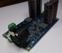
A simple, single-channel, low-cost, high-efficiency, high-performance audio class-D power amplifier I designed and constructed some years ago for experimentation and personal domestic use.
Most of the components can be SMD, except for connectors, large capacitors and perhaps power inductors.
A differential to single-ended input buffer allows both balanced and ground referenced audio inputs.
The fully differential configuration of the PWM modulator, the MOSFET power stage and the feedback network, produces low distortion (particularly on even harmonics) and simplifies supply to a single 6 to 24Vdc (3A minimum). Supply can be obtained from a simple mains transformer + rectifier bridge. The rest of supply voltages are generated internally.
Based on a simple self-oscillating architecture, the modulator (an ultrafast comparator) varies not only the duty-cycle of the PWM signal but also its frequency in response to output voltage error, in order to maintain this error below a fixed limit. The varying frequency helps to keep radiated EMI below acceptable limits.
The default gain is 10, but can be modified changing R11 & R21.
Two prototypes have been working for years without problems as a stereo PC audio amplifier.
As a future improvement and in order to get a fully differential signal path implementation, the input buffer could be replaced by a differential input/output device.
Supply: single 6 to 24Vdc
Input impedance: 22kohm
Bandwidth (-3dB): 7Hz - 70kHz
Default gain: 10
Max. power on 8 ohm speaker (4.4Vpp sinewave input): 30W
Discussion (9 comments)

inOr 8 years ago
"Most of the components can be SMD.." You mean that through-hole equivalents are available, and can be used with a.) your board or b.)user-constructed board?
Reply

sequencer 8 years ago
My design of the PCB was aiming to get a compact size and a good behaviour regarding HF stability, and hence audio fidelity. Costs of components and PCB were also considered, so the choice of components is SMD where possible (i.e. except for connectors and bulk electrolytics).
Given that power inductors have a manifest non-ideal behavior (hysteresis, saturation, parasitic resistance and capacitance), in my board these components can be mounted as through-hole as well. There are holes for this purpose in their pads, intended to be a way for experimentation with different types of inductors. So the power inductors are the only SMD components that can be T/H in my board.
Regarding PCB layout considerations, needless to say, when the circuit is working, digital power lines with very high slew-rate transitions are present in the proximity of high bandwidth devices.
These facts lead to a careful HF PCB layout: analog part must be separated from digital, and high current PWM tracks as far as possible from everything and sorrounded by ground areas. Shortest tracks and a good ground plane are mandatory, as well as plenty of vias connecting top side ground areas to bottom ground plane.
Observing these points, I'd say is perfectly possible to do a T/H version of the circuit, but not with the same IC references: THS4531, MCP14628, IRF8313 and TL3116 can only be found in SMD packages. Sorry.
Of course, all resistors, capacitors and diodes could be T/H, as well as the 7805 voltage regulator. Regarding the comparator, an AD8561 in PDIP8 would probably do the job with few modifications, if any.
No replacement problems either for power MOSFETS and their drivers. There's infinity of alternatives. Apart of voltage, current and gate capacitance specifications, keep in mind the rise and fall times to avoid cross-conduction, and provide switching dead-time if necessary.
I couldn't find a T/H replacement for the fully differential input amplifier THS4531. I think the best solution in this case would be a dual RRIO opamp.
Reply
Show more
1 Comment(s)


Calpe 8 years ago
The PCB is available from where?
Reply
sequencer 8 years ago
Sorry Vincent, there's no definitive PCB. I did a first PCB (shown in the photo) on which I tested the concept and improved on the initial design, consisting this improvement basically on some simplification, by eliminating an unneeded opamp, wired a couple of jumps and tried different power inductor types, to arrive to the version published in the schematic.
After this, I just hadn't the time to continue the project. Now a couple of working prototypes remain, and some other ones stored somewhere.
If enough interest, maybe I could elaborate a better PCB.
Thank you very much.
After this, I just hadn't the time to continue the project. Now a couple of working prototypes remain, and some other ones stored somewhere.
If enough interest, maybe I could elaborate a better PCB.
Thank you very much.
Reply
Show more
1 Comment(s)

Ravindra M. Desai 8 years ago
With this reference design you have taken the complexity out of the fully differential configuration of the modulator and MOSFET stage. This is very scalable. A look into Si824x driver will allow the user to play with dead-time setting and strike a right balance of THD + N vs Efficiency.
For a hobbyist, this design is nice and simple. Thanks for sharing!!
Regards,
Ravindra.
P.S. Read U6 GND pin as pin-6
For a hobbyist, this design is nice and simple. Thanks for sharing!!
Regards,
Ravindra.
P.S. Read U6 GND pin as pin-6
Reply
Show more
1 Comment(s)

Updates from the author
sequencer 8 years ago
In my audition test setup, a pair of them are supplied directly from a toroidal mains trafo (18 + 18 Vac secondary). The audio input comes from a Creative Sound Blaster Audigy 24-bit sound card. The outputs connect to Polk Audio speakers.
Playing 24-bit hi-res, good quality recordings in FLAC format files, the system sounds spectacular, even with low-cost components, especially the inductors, which contribute the biggest part of THD.
Remember that single ended stereo signals must be converted to 2 differential signals, one for each channel. Connecting a stereo signal to the amplifier can produce strange artifacts or absolute silence if the signal is mono.
Thank you.
Bill of materials (10kb)
3D view of the PCB with components (4025kb)
CAD files for PCB service (72kb)
PCB printouts (703kb)
harmonics at +6dBV 1kHz input, 28Vdc supply, output 11W (187kb)
Ravindra M. Desai 8 years ago
Connecting a stereo signal will in-fact produce un-processed surround (L-R or R-L). It can be best enjoyed with another channel producing Center (L+R) signal.
Again, Luis, finding IRF8313 and using it in this application was simply brilliant.
Merry Christmas and best wishes for a happy new year!
Regards,
Ravindra.
sequencer 8 years ago
Best wishes and a Happy New Year.
sequencer 8 years ago
At the initial trials I had some troubles keeping under control the 200GHz gain-bandwidth product of the TL3116. I achieved it with a little of positive feedback (that's what all we need). Now I'd say the main goals are fulfilled.
During the next days I'm going to take more measurements and try tuning on some component values. Then I'll post the complete design with files and graphs.
Thank you.
THD+N at 25Vdc (Vi=-10dBV) (168kb)
dsc-0271.JPG (326kb)
Ravindra M. Desai 8 years ago
Impressive results, especially at low power levels. I look forward to the tweaks.
Any parameter of TL3116 is different than the earlier comparator that needed changes to feedback factor?
Thanks and regards,
Ravindra.
Boo 8 years ago
Very nice design. Ik looks great.
Please post the schema and pcb design if you are ready.
Thanks,
Berto.
sequencer 8 years ago
So, in order to stabilize the TL3116, a small capacitor connects one of the inputs to its output, generating a small level of hysteresis that cleans up those state transitions.
Or if you prefer, by means of this feedback capacitor the output transition produces a fast change at the input, as expected by the comparator.
As a comment, another significant feature, the typical input offset voltage, is tighter in the TL (0.5 mV vs 1mV), which is desirable in our application because input offset voltage is seen at the amplifier output multiplied by the amplifier gain, in our case 10.
sequencer 8 years ago
As input connector it's ready to accept an XLR or a TRS jack, at user's choice.
For the input stage, I finally decided to use a fully differential amplifier THS4531.
Attached a screenshot of the 3D view. The 3D step model can be seen at http://a360.co/2cyN932.
sequencer 8 years ago
Another point is the possibiity of using a full differential amplifier (FDA) for a full differential signal path. Or what kind of audio input connector (TRS female jack?) can be used for both balanced and single-ended sources.
Ravindra M. Desai 8 years ago
1. I like the idea of using the power-supply (bridge + bulk caps) on the same PCB.
2. Yes, let's add a fully differential amplifier/ buffer at the front to allow fully differential signal path. How about an OPA1632 or LME49724?
3. We can use an XLR female, PCB mount connector for landing the input signal. The suggested part # is Neutrik NC3FAAH1.
4. Are you planning to change the output section? If yes, kindly do consider Si8244 driving either 2 x IRFI4020H-117P or 4 x IRFB4127
5. How about using Epcos RM14 N87 to wind both the output inductors on the same core. It will be sturdier mount and will occupy almost the same area on the PCB?
6. Do we need a DC servo? Should we consider more features such as a limiter?
7. Should the new design be through hole except for the ICs?
Do let me know how I can help. I will understand even if you completely disregard all the above. Its your design!
Regards,
Ravindra.
JohnHind 8 years ago
Calpe 8 years ago
sequencer 8 years ago
First some general comments about the project. The aim of this re-design is to do it cheaper, smaller and electronically simpler, almost minimalist, making it easy to build, while trying to get a more than acceptable quality. No hazardous voltages, let's say 24V max. so anybody can play with it.
In this way the first step is to replace the comparator. The second, to get rid of the -5V inverter. I think this is unnecessary and the signal devices can be supplied with just a single +5V or +6V regulator.
Other modification I propose is to avoid electrolytic caps except for the bulk ones. All 1206 MLCC ceramics.
Ok, going to your ideas:
The FDAs you mention are excelent devices, but apart of their high cost, I see the drawback of a reduced output swing.
With a single +5V and taking into account the limited input common mode of the comparator, the FDA should have near rail-to-rail outputs.
We could use the THS4531 instead. Anyway, why not using a dual RRO opamp instead? The final function is nearly the same and the user could choose among a lot of pin-for-pin compatible devices.
For example OPA2725. Let me know your opinion.
XLR connector: I think it's ok.
About the output section, the present IRF8313 has the unusual quality in a MOSFET of having a total turn-off time shorter than its turn-on counterpart.
So, no need of dead-time control, simplifying a lot and improving reliability. Drawback: low voltage. In a future version with higher power the Si8244 will fit perfectly.
And if you know of another power MOSFET turning faster off than on...
Epcos core: I don't know. I had thought of a pair of off-the-shelf SMD inductors, for example Bourns SRP1265A-100M. Easy and cheap.
I have to consider your other suggestions, but for the moment I don't see a real benefit on more advanced features.
Regarding technology, SMD vs T/H, well I personally prefer SMD. It's cheaper, smaller and has better performance in high frequency than T/H.
At the end of the day the design effort is pretty the same. I'd use everything 1206 and SOIC8, I think it's not so hard to solder, even with a solder iron and no SMD oven. I'm open to opinions.
If this redesign works ok we'll develop a more powerful and sophisticated version.
sequencer 8 years ago
Or are you thinking of a system based on a Digital Signal Controller with HRPWM capabilities, like those used in motor drives?
Ravindra M. Desai 8 years ago
After reading through your thoughts (thanks for the design details!) I completely agree with you to keep this re-design minimalistic. A bare minimum design excites me just as much.
I did debate over TH vs SMD (because this is DIY) and there too I agree with you that SMD is needed for the application.
Lastly: full credit to you for the IRF8313!!
I look forward to v2.0.
Thanks and regards,
Ravindra.
JohnHind 8 years ago
sequencer 8 years ago
I saw this evolution a couple of years ago and I'm working on a proof-of-concept board. But this is much more complex and harder than the present project.
The software of the DigAmp is the most important part, becoming basically a Software Defined Amplifier.
sequencer 8 years ago
Calpe 8 years ago
sequencer 8 years ago