

Crypto Dev Shield for "ZMC" Zilog Z80 system
May seem like just some nostalgic 1980s retro system, but in fact it is: 1.) A versatile platform for learning assembly programming on the lowest level and even more important, 2.) A good platform for development of ultra-secure crypto systems!
This is another sequel in our highly-secure communication systems series! I suggest you to first watch our interview here:
https://www.elektormagazine.com/news/secure-communications-an-interview-with-luka-matic
where the most of the problems of today's secure systems design engineering are explained. Please pay special attention around 40:38 when we talk about methods of using "retro" technology to increase security. There we refer to one particular Zilog Z-80 system:
http://www.sunrise-ev.com/z80.htm
which is very simple and especially convenient for implementation for even more secure systems than those that we previously implemented using Atmel AVR and Arduino.
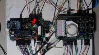
Since I grew up with Sinclair ZX Spectrum, and got well acquainted with Zilog Z80, first I decided to buy the ZMC main board PCB along with FP PCB (front panel-LED 7-seg display and keyboard) on the aforementioned web site. After assembling the PCBs and first power-up and testing, I quickly got truly impressed!
It is really amazing what Lee Hart managed to squeeze into only several kB of UV EPROM, leaving 88% of CPU time and cca. 70% of EPROM and RAM for further development!:
-machine code monitor, capable of monitoring and single-stepping of both RAM and ROM (with timer-interrupt triggered single-stepper)
-software bitbanged keyboard scanner, 7-char-7-segment LED + 7 extra LEDs display driver and duplex 9600 UART port (to work with the front panel on the photo attached)
-SRAM bootloader - load your assembly or BASIC code through UART and start the program!
-a simple 16-bit integer BASIC interpreter, capable of accessing IO ports, peeking and poking through the memory, and calling assembly-code subroutines
-there is also another PCB add- on made by Lee Hart, with up to 512kB of bank-switchable RAM, one more hardware UART and SD card interface as well !
So this is a miniature, Arduino-size system, with 32kB UV EPROM and 32kB SRAM, to fully exploit all the capabilities of Z80, connect it to all sort of periphery devices and utilize all the advantages and flexibility of Von Neumann's compared to Harvard's architecture.
----------------------------------------------------------------------------------------------------------------------------------
In order to use this system for any cryptography- related stuff, I decided to design another "shield" for this system. I wrote the assembly code for all the CTC, UART, I2C and 1-wire bus comms routines and tested them all. These are all the features:
-Z80 CTC (4-channel counter-timer) - precise hardware timing is necessary for good encrypted communications. I used UB857D, its East German clone, also produced in millions and still easily available because I didn't have any original CTC handy. Assigned the IO addresses to 0x00, 0x01, 0x02 and 0x03 to make it compatible with the rest of the Altoid PCBs.
-74HC138 (3-to-8 decoder), for extra IO channels , one more 8-bit input port (74HC245) and one more 8-bit output port (74HC273 latch) - also used to bitbang I2C port, 1-wire port and one more UART port on my board, and anything else . IO channel 0x04 for 74HC245 (input) and 74HC273 (output), and IO channel 0x06 for reseting the watchdog timer.
-DS1307 RTC on I2C port, with CR1220 battery that can keep the clock running for several years
-AT24C serial I2C EEPROM - useful for many things, like quick dumping and restoring SRAM contents
-DS18B20 one-wire bus thermometer - can't do secure cryptography without one :)
- 74HC74- watchdog timer, RC analog, adjustable with a 1meg trimmer in a span of cca. 0.5-7 seconds. Can activate NMI interrupt, or RESET, configurable by jumpers. WDT is reset by writing to IO 0x06.
-another 74HC74 -featuring a code-injection protection circuit (!):
Having all the address, data, IO and control signals easy to access, all the firmware in UV EPROM, all the units physically separated, old and reliable hardware tested for more than 30 years, this system is more secure than any modern highly-integrated MCU or FPGA... except for one thing. Because of its von Neumman's architecture it is more susceptible to any kind of buffer-overflow attacks (code-injection, stack-smashing, runaway code, remote reset , illegal opcode...). Executing a code from SRAM may be useful for testing during development, but for any secure crypto application the fully tested version of the program must be stored exclusively to UV EPROM, while SRAM can be used to store only data, not program. So , a simple circuit built around this IC detects any attempt to execute a code from SRAM, and reacts immediately.
Updates from the author
lux36 4 years ago
1.) All the IO channels on Lee Hart's modules have the IO addresses with A6=1. My IO units use channels 0,1,2,3 (four CTC counter-timer channels, addressed with A1 and A0 while A2,A3 and A6 must all be at 0), 4 and 6 (CH4 "read"-from IC2 inputs, CH4 "write" to IC3 outputs, CH6 "write"- to reset the WDT, A2=1, A3=A6=0). I also added A3 (must be at 0 for all these channels) for possible future upgrades.
2.)CON1 and CON2 are pinheader connectors. Big circles (like e.g. between CON1 and IC2, or also at bottom right side of IC8-CTC) are DIP (in fact SIP) sockets where jumper wires can be inserted- nothing beats the security of "programming" with jumper wires- this can't be "reprogrammed" by a code injection attack :)
3.) If made with a combination of SMD and THT, it can be "sandwiched" between the main board and the FP board (front panel - LED display and a keyboard). The 26 pinheader connections listed on the top right of the schematics are used stacked on the left and right side of the Shield PCB, while aforementioned (CON1 and CON2 - additional 8XIn and 8XOut) are placed on the top and bottom of the PCB. Check the mainboard schematics attached to compare.
4.)I2C and 1-wire interface are implemented on I0-Q0,I1-Q1 and I2-Q2, each can be connected/disconnected using JP1-JP6 as needed. One more UART (called "CTC-UART" because CTC IC is used to clock it) is available on I7-Q7, through JP7 and JP8. Additional I2C and 1-wire devices can be easily added to the system - just connect them in parallel on the respective bus.
5.)Capacitors C5,C6, and C7 can have different values depending on the 32.768kHz XTAL used. Use C7 to trim the frequency to exactly 32.768kHz. SQW/OUT can be programmed (with I2C commands) to output 32.768kHz, 8.192kHz, 4.096kHz or 1Hz squarewave. This output can be connected (with a jumper wire) to e.g. TRG0-TRG3 pins on CTC for precise timing/counting.
6.) IC1 is a 32kB serial EEPROM which can back up entire RAM if needed.
7.) IC5 (A and B) is a watchdog timer. Can be adjusted using R10 in a span of cca 0.5 to 7 seconds. Writing to IO CH6 creates a 0.5us pulse on CLK input of IC5A. R8 and C9 extend it to several milliseconds on the output of IC5A to ensure the discharge of C10 (a WDT reset). If the WDT times out, LED1 is lit and /NMI is activated (if enabled by JP9 jumper and S1 switch). Pushing the S2 "/RESTORE" button will reset the IC5/IC6 protections without resetting the system.
8.) Because of electrical properties of /NMI input on different types (i.e. NMOS or CMOS) and manufacturers of Z80 ICs (tested several brands including the East German Cold War clones), the R20-C11 circuit is put in place to ensure that /NMI is swung low enough (around 0.1V) for at least 200ns - although 0.6V should be enough for TTL-like inputs, some types failed to react and this must be prevented at all costs.
9.) IC6 is a protection added to remedy the main weakness of Z80 - because of its Von Neumann's architecture, it is highly susceptible to buffer overflow-code injection attacks. IC6B will trigger the /NMI if /RAM and /M1 go low simultaneously - this indicates an attempt to execute an instruction fetched from RAM. Normally, for any secure cryptography application, the code is executed from ROM, and RAM is used only for data storage. An attempt to execute a code from RAM can surely be considered as a code-injection attack underway. Similarly to this, IC6A will trigger if a program tries to write to ROM. This is also an indication of a code-injection attack- since an attacker usually doesn't know the exact memory location of the targeted system, usually a long string of NOPs ( a so called "NOP sled") is usually injected before the attack code payload. This can easily wrap around the end of RAM to the beginning of ROM. Writing to ROM can't do any harm by itself, but this way the protection will prevent the execution of injected code even before it starts!
10.) R17, R18, and R19 will pull the data lines D3, D5 and D6 high or low if data bus is in high-Z state - this is done by reading from any non-existing IO channel (I used a "read" from IO channel 6 - its Y5 output on IC4 decoder is not connected to anything, so the data bus will remain in high-Z state). This is used to read the "NMI signature" displayed on terminal in case that /NMI ISR is activated.
11.) On "demo terminal screenshots" you can see both UART ports operating simultaneously- the one of Lee Hart's FP board (green-on-black Teraterm, COM63) and my CTC-UART (Br@y's grey terminal on COM64). My demo program is burned to UV EPROM, starting at address 0x3700, while Lee's main firmware (with machine code monitor, single stepper, FP keyboard scanner, LED display driver and everything else) starts at 0x0000 and ends at 0x364C. You can see the command "GO 3700" which starts my demo. My demo first tests my UART and then it can execute different I2C and 1-wire commands from my UART to test IC1, IC7 and IC9. One special command will send it to a mode to constantly display time and date (read from IC7) and temperature (read from IC9), both on Br@y's terminal and FP LED-display. Since LED display is bitbanged by a routine from Lee's firmware which is first loaded to RAM and then executed from RAM, it activates the "RAM exec alarm", so this alarm was disabled in my demo videos by removing the JP11.
12.) After I simulated the WDT overflow by reducing the WDT time constant below 1 second (see the video), the NMI ISR was activated (see the terminal screenshots). After disabling the maskable /INT interrupts, the NMI ISR routine displays the SP, dumps the top of the stack, shows the NMI signature (0x46 is consistent with "WDT overflow" and "RAM exec"activated) and offers an option to erase RAM (if you want to perform a "cold restart" without disconnecting the power), and starts a demo of IM2 interrupt mode on CTC. It can easily be configured also to e.g. dump entire RAM contents to IC1 EEPROM for further analysis (e.g. to try to identify the injected code).
13.) The NMI ISR can also be activated by pushing the S3 button. Analyzing the stack dump you can identify how many times the button bounced - how many consecutive calls to NMI ISR were made - there is a debounce routine at the beginning of the ISR. None of the alarms were active (this part of the code is executed entirely from ROM, so "RAM exec" alarm could be reset by "/RESTORE" button), so you can see the signature was 0x7E.
---------------------------------------------------------------------------------------------------------------------------------------------------------
My software is just a demo, to show that this shield can be used for development of a secure crypto system - which would probably have to be implemented without the FP board (keyboard and LED display), because the code required to drive it is not secure enough.
Z80MC_crypto_shield.pdf (44kb)
demo-terminal-screenshots-20200708123521.png (189kb)