

Power Analyzer
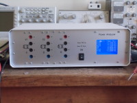
1, 2 or 3 channel power analyzer, giving number or graphic display (scope picture or FFT) on a 128 x 64 LCD
This project was inspired by the Power Meter published in Elektor Magazine in September 2015. At first sight I thought it was very interesting and I wanted to make one myself. But reading further on I found some limitations and drawbacks. So in the end I decided to start with an "improved" design.
Things I wanted to improve were:
The above means that the input and amplifier circuit need a big redesign. Also a uP is needed at the hot-side, to make the offset correction and auto-ranging possible.
The Main board is not very original. The idea is to use a 128 x 64 GLCD as used in the EasyPIC7 development board for display and for control I use also the touch panel. So the biggest part of the main board is a copy of the circuits of the EasyPIC7 board. On top of the circuit diagram there is a square wave oscillator, which generates a square wave of 12 Vpp at a frequency of about 150 kHz. This signal is used to power the Satellite boards. The communication with the Satellite boards will be via I2C. The uP on the main board will be the master, the satellite boards are the slaves. The connectors to the satellite boards are at the right of the diagram.
The Satellite boards deviate a lot from the original in Elektor. I start with the input circuit, at the far left. I wanted to measure voltage and current independently. This is not fully realizable, but with the given circuit the low voltage input and het current input can float about +/- 1 V with respect to each other. This is realized by the diode D3, D4, D7, D8. Without measures taken, the circuit can be blown up by a wrong connection: the high potential to the low voltage input and also the current input at the low voltage side.
To prevent damage the circuit with T10 …T14 and reed relay K1 is added. A first current limitation is realized by R11: at 750 V input voltage the maximum current is 0.5 A. If the current through R11 is larger than some 10 to 20 mA, there will be a small current through R34, which is detected by T11 and T13. This will trigger the thyristor circuit with T10 and T12. Once triggered the thysistor circuit will remain in this state and it will switch off T14 and K1. Signal OC indicates to the uP that the protection has been triggered.
When there is no power K1 is also switched off (V-low is disconnected), so then the circuit is safe.
To restore operation the power of the circuit has to be disconnected and connected again.
The voltage divider gives 100 mV output at the maximum input voltage of 750 V (DC).
The maximum AC voltage will be about 500 V.
The current sense resistor is now 6.5 mΩ to give about 100 mV at 15 A-DC (about 10 A-AC).
The amplifiers for voltage and current are equal. I describe only the voltage amplifier (on top). T1, T2 and T4, T6 form switches which connect the differential amplifier either with the signal from the input circuit or short the input to make offset measurement possible. The value of the offset can be stored and subtracted later from the measurement to make a “clean measurement” possible.
The amplifier is a common instrumentation amplifier. T3, T5 switch the gain of the first stage to either 1x or 25x. IC5 makes the differential signal single ended. The last stage with IC4 can switch the gain to either 1x or 5x. So there can be four gains: 1x, 5x, 25x or 125x. The gain setting will be under control of the uP. The amplifier will generate a positive or negative signal with respect to COMV. This signal is 0.5 times VREF, which is generated by the circuit on the top right of the circuit diagram. VREF is 4.5 V, so COMV, COMI and CINV are 2.25 V. VREF and CINV are connected to the ADC of the uP. The ADC of the used PIC18F26K80 can convert to 13 bits when used in the indicated way (12 bits plus a sign bit). For 750 V this gives a resolution of about 200 mV / bit. For 6 V about 1.6 mV/ bit. I consider this as sufficient for this purpose.
Before sampling, the signal needs to be filtered, the cut-off frequency has to be 2.4 kHz. The roll off is maybe an issue. I have chosen for a combination of four first-order filters. When calculated for 3 dB attenuation at 2.4 kHz the attenuation at 5 kHz is only 0.32 (about – 10 dB). It is questionable whether this is sufficient.
The square wave coming from the main board is fed to the transformer at the right (ratio 1:1). The rectifiers give then an output voltage of something less than 6 V. With parallel regulators this is controlled to +/- 5 V.
The windings of the transformer have an isolation value of 900 V, so the total isolation will be 1800 V peak, provided that the rest of the construction is OK. The I2C signal will go via IC14, which has an isolation value of 4 kV peak. So the satellite board will be completely floating with respect to the main board and with respect to each other.
So far about the circuit diagrams. I now have to write some software
Things I wanted to improve were:
- The input circuit: It should be possible to measure current and voltage independently from each other: the current through the connecting leads shall not influence the voltage reading.
- The sampling rate: the low sampling rate makes it only possible to measure the first 8 harmonics of a 50 Hz signal (with perfect filter). This should be increased to the first 40 harmonics.
- Range switching: The used method was a bit clumsy and also risky: Suppose that you are measuring at a 230 V circuit and has to make a quick adaptation... The range switching shall be made automatic.
- Offset correction: this shall also be automatic.
The above means that the input and amplifier circuit need a big redesign. Also a uP is needed at the hot-side, to make the offset correction and auto-ranging possible.
2016-06-09
The intended block diagram is given in the drawing at the top of this document. There will be a main board and three satellite boards. The preliminary circuit diagrams are given in the attachments. At the moment of writing, nothing has been tested yet.The Main board is not very original. The idea is to use a 128 x 64 GLCD as used in the EasyPIC7 development board for display and for control I use also the touch panel. So the biggest part of the main board is a copy of the circuits of the EasyPIC7 board. On top of the circuit diagram there is a square wave oscillator, which generates a square wave of 12 Vpp at a frequency of about 150 kHz. This signal is used to power the Satellite boards. The communication with the Satellite boards will be via I2C. The uP on the main board will be the master, the satellite boards are the slaves. The connectors to the satellite boards are at the right of the diagram.
The Satellite boards deviate a lot from the original in Elektor. I start with the input circuit, at the far left. I wanted to measure voltage and current independently. This is not fully realizable, but with the given circuit the low voltage input and het current input can float about +/- 1 V with respect to each other. This is realized by the diode D3, D4, D7, D8. Without measures taken, the circuit can be blown up by a wrong connection: the high potential to the low voltage input and also the current input at the low voltage side.
To prevent damage the circuit with T10 …T14 and reed relay K1 is added. A first current limitation is realized by R11: at 750 V input voltage the maximum current is 0.5 A. If the current through R11 is larger than some 10 to 20 mA, there will be a small current through R34, which is detected by T11 and T13. This will trigger the thyristor circuit with T10 and T12. Once triggered the thysistor circuit will remain in this state and it will switch off T14 and K1. Signal OC indicates to the uP that the protection has been triggered.
When there is no power K1 is also switched off (V-low is disconnected), so then the circuit is safe.
To restore operation the power of the circuit has to be disconnected and connected again.
The voltage divider gives 100 mV output at the maximum input voltage of 750 V (DC).
The maximum AC voltage will be about 500 V.
The current sense resistor is now 6.5 mΩ to give about 100 mV at 15 A-DC (about 10 A-AC).
The amplifiers for voltage and current are equal. I describe only the voltage amplifier (on top). T1, T2 and T4, T6 form switches which connect the differential amplifier either with the signal from the input circuit or short the input to make offset measurement possible. The value of the offset can be stored and subtracted later from the measurement to make a “clean measurement” possible.
The amplifier is a common instrumentation amplifier. T3, T5 switch the gain of the first stage to either 1x or 25x. IC5 makes the differential signal single ended. The last stage with IC4 can switch the gain to either 1x or 5x. So there can be four gains: 1x, 5x, 25x or 125x. The gain setting will be under control of the uP. The amplifier will generate a positive or negative signal with respect to COMV. This signal is 0.5 times VREF, which is generated by the circuit on the top right of the circuit diagram. VREF is 4.5 V, so COMV, COMI and CINV are 2.25 V. VREF and CINV are connected to the ADC of the uP. The ADC of the used PIC18F26K80 can convert to 13 bits when used in the indicated way (12 bits plus a sign bit). For 750 V this gives a resolution of about 200 mV / bit. For 6 V about 1.6 mV/ bit. I consider this as sufficient for this purpose.
On the sampling rate and filtering
I want to measure the first 40 harmonics from a 50 or 60 Hz signal. So the highest frequency is 2.4 kHz. The minimum sampling rate has then to be 4.8 ks/s, but 7.5 or 10 ks/s is better. The uP has then to make 15 or 20 20ks/s (for voltage and current). The PIC18F26K80 needs a minimum of 17 µs for one conversion, so a maximum speed of 58 ks/s is possible. (forgetting the time needed to work with the acquired data). So the speed does not seem an issue.Before sampling, the signal needs to be filtered, the cut-off frequency has to be 2.4 kHz. The roll off is maybe an issue. I have chosen for a combination of four first-order filters. When calculated for 3 dB attenuation at 2.4 kHz the attenuation at 5 kHz is only 0.32 (about – 10 dB). It is questionable whether this is sufficient.
The square wave coming from the main board is fed to the transformer at the right (ratio 1:1). The rectifiers give then an output voltage of something less than 6 V. With parallel regulators this is controlled to +/- 5 V.
The windings of the transformer have an isolation value of 900 V, so the total isolation will be 1800 V peak, provided that the rest of the construction is OK. The I2C signal will go via IC14, which has an isolation value of 4 kV peak. So the satellite board will be completely floating with respect to the main board and with respect to each other.
So far about the circuit diagrams. I now have to write some software
Discussion (4 comments)

michael zheng 8 years ago
Great article and a good design. Can you tell us how much is for the material cost without enclosure?
Also there are exisiting power measurement DSP chips, why did you choose to use uP + components to do it? Concern about cost or performance about DSP chips?
Michael
Also there are exisiting power measurement DSP chips, why did you choose to use uP + components to do it? Concern about cost or performance about DSP chips?
Michael
Reply
Show more
0 Comment(s)

JohnHind 8 years ago
Seems to me that modern instruments should consider using a Tablet for display and UI - either build one into the box, or preferably just serve the measurements over BLE so one tablet can be used for multiple instruments.
A tablet will give a much more capable UI and Display and probably actually costs less than a dedicated display, even if the tablet is dedicated to just this one function. If you use BLE, you get galvanic isolation for free and can make the entire instrument "hot side". Plus you get hardware capable of networking, logging, integrating multiple instruments ...
A tablet will give a much more capable UI and Display and probably actually costs less than a dedicated display, even if the tablet is dedicated to just this one function. If you use BLE, you get galvanic isolation for free and can make the entire instrument "hot side". Plus you get hardware capable of networking, logging, integrating multiple instruments ...
Reply

Wil Dijkman 8 years ago
Hello John,
Thanks for your reaction. For every design you have to make choices and to struggle with limitations. My limitation is that I do not know enough about programming a tablet. I am working on the logging, it can work in the present design with the limitations of the small display.
Your idea is certainly interesting. Feel free to propose the needed additions and write the needed software.
Thanks again for your reaction.
With kind regards
Wil Dijkman
Reply
Show more
1 Comment(s)


wim.cranen@wccandm.nl 8 years ago
Hi,
This looks like a very interesting project.
I have some questions:
- are you planning to implement a more detailed screen to display the results?
- Is a crest factor calculation implemented?
- How does the equimpment compare to a lets say C.A 8335 of 435-II?
If you feel these questions are absurd or of less importance, please say so.
I don't want to consume your time.
Grtz, Wim
Reply
Wil Dijkman 8 years ago
Hello Wim,
Thanks for your reaction.
Your questions:
On short notice no other screen. For graphics the display is indeed rather limited, but for numbers it is OK.
Crest factor is now not included, but can easily be added. Please wait for the next software update.
I do not know the instruments that you mention. I believe they are comparable, but to what degree, I do not know.
with kind regards
Wil Dijkman
Reply
Show more
1 Comment(s)
Updates from the author
Wil Dijkman 4 years ago
EMMANUEL VIRATEL 4 years ago
Best regards,
Emmanuel (TOULOUSE-FRANCE)
mail: viratelemmanuel@yahoo.fr
Wil Dijkman 4 years ago
Wil Dijkman 4 years ago
Wil Dijkman 4 years ago
EMMANUEL VIRATEL 4 years ago
I'm Emmanuel, an electronic student from FRANCE. I'm very interested by your power Analyzer with two PICs.But when i've dowloaded the mikrobasic code there is no .mbas file and i can't see the source code
Pleased would you send me the complete folder with the .mbas file
My email is viratelemmanuel@yahoo.fr
Thanks a lot for your quickly answer,
Emmanuel
Wil Dijkman 4 years ago
Wil
Wil Dijkman 6 years ago
By co-incidence I detected an error in the POWERANASATTELITE.mbas program.
It concerns line 300. This reads:
while ADCON0 = 1
It shall read:
while ADCON0.1 = 1
The effect of this error is that the offset of the current channel is not well measured and it will also influence successive measurements. It might be the explanation for the noise that I encountered and never could explain.
I did not test yet this correction. This will be followed up a.s.a.p.
(I am busy with another project now and it might take a few weeks before my workbench is empty again).
Wil Dijkman 7 years ago
I have adapted the software for the main board. The changes are:
On the logging function: When entering this function you first have to choose the time period that you want to apply. You can choose between 0.25 h and 128 h in steps of a factor of 2 (ten possibilities). Next step is choosing how many traces you want to log (maximum is 3) . Each trace can be coupled to a channel and from that channel you can choose either V, I or P.
If the signal frequency is 50 Hz or higher, then it is considered AC, else DC.
Pressing Continue immediately starts the logging. You will enter the numeral screen, where you can watch the average value, maximum and minimum. And the elapsed time. You can also go to the graphical screen. Above the screen you can select another trace, if it is switched on.
Pressing Return brings you back in the main screen, the gathered data are lost.
Crest factor (V-CF or I-CF) you can select in the configuration screen. It simply divides the highest peak value (positive or negative) by the RMS-value of the signal. Remember that the bandwidth of the measuring amplifiers is 2.5 kHz, so this function is not suitable for audio. Only until, say 250 Hz depending on your taste.
Herewith I consider this project as finished. There will be no more large additions or changes. But of course I will answer any questions.
Wil Dijkman 8 years ago
The satellite board: There is one addition, a test pin on RC5 of the uP. This test pin is needed for alignment.
Software for the satellite board: This is adapted. The sampled signal is now digitally filtered before sub-sampling. This is to decrease aliasing.
The filter is added to the sub-procedure “verwerksamples”. It has a bandwidth of about a quarter of the sampling period, so 2.55 kHz in the frequency domain.
The filter is based on chapter 16 of The Scientist and Engineer's Guide to Digital Signal Processing
By Steven W. Smith, Ph.D.
http://www.dspguide.com/pdfbook.htm
The Blackman-window is used and the filter has 13 coefficients (M=12).
The choice of the length of the filter is a compromise between calculation time, needed memory and performance (= suppression of signals above 2.55 kHz and attenuation of signals below 2.55 kHz).
The mainboard
I have changed my mind about the connection with the PC. After all I cannot think for a good use of it, so the components are left out.
The supply section is adapted: it is now possible to use either a 12 V stabilised or a 15...18 V supply without stabilization. The selection can be made by a solder joint. (SJ1).
There are two other solder joints: MAX1 and MAX2. With these the number of channels can be given to the uP: closing MAX1 only means one, closing MAX2 means two and closing both means three channels. A lot of bridge wires are added to make it possible to use a bi-layer board.
How to build together
A front plate has been designed (for a three channel version), which can be ordered at Schaeffer. I used a metal housing (order code 1510827at Farnell, manufacturer Metcase, M5503110).
See the photographs.
How to connect. This is indicated in the figure PowerAnaConnections.png. It makes a difference whether you measure the consumption of a load or the supplied power from a source. With the indicated methods the voltage drop of the connection leads and the current measurement section is eliminated. The voltage difference between the I connections and the V- connection shall remain below 0.5 V. Otherwise the protection is addressed and the power supply has to be cycled.
How to use
After switching on, the Measurement screen appears. It displays some units and their values for the chosen channel. At the top of the screen you can choose another channel (if it is available).
The screen can display maximum 7 units. Which units, you can adjust at the Configuration Screen
First go to the Main Menu (top right of the screen) and then choose Configuration. The Configuration Screen appears with 16 units to choose from. The chosen units are highlighted; there will be at maximum 7. If you want to change the displayed units in the measurement screenand the maximum has already been reached, then first de-highlight another unit before you make your choice. Some units will go without saying but some will need explanation.
Vdis and Idis (distortion): This is calculated according:
(Sorry! something went wrong with the formula!)
Vdis = (sqr(sum for N=2 to N=40 of square(VN))) / V1
where VN stands for the amplitude of harmonic N of the signal.
Re-P means real power, P-VA means Vrms x Irms, Im-P means imaginary power, and PF means power factor = Re-P / P-VA.
If you choose Eff-> then you will come into the Efficiency Screen. Here you can choose the formula which describes the power relation that you are investigating and then you go back to the Configuration Screen. If you go back to the Measurement Screen, the chosen formula with the calculated value is displayed for all channels.
Back in the Configuration Screen you can also choose for Graphs->
Pressing this you can choose between “Scope” or “FFT”.
Press Scope. This brings you to select traces. You can select a trace by pressing on it. Trace1 will always be on. A selected trace will be high-lighted. All traces can be “connected” to a channel and to V, I or P of that channel. The display will be “triggered” by the positive zero crossing of trace1. The display will give you an impression of the wave shape of the signals and their mutual phase relation. You will always see two periods. In fact only one period which is repeated once. The amplitude of the signals is always the same: voltage signals have the maximum amplitude. To distinguish them from voltage signals, current signals are displayed with a 20 % lower amplitude and power signals at 60 % amplitude. See for an example the waveforms of a transformer which goes in saturation. So the “scope” has no measurement function, only an indication of shape and phase relation.
Once more in the Graphic Screen, press FFT. This shows the FFT components of a selected signal. On top of the screen you can select the channel, LINear or LOGarithmic display and either V or I.
The largest harmonic (usually but not necessarily the first harmonic) is displayed at 100 % or 0 dB.
The horizontal scale gives the number of the harmonics, so no frequency.
From the Configuration Screen you can also go to Logging->. This is at this moment still under construction.
How to adjust
From the Main Screen you can go to the Calibration screen.
You can choose between calibrating the screen and calibrating the channels.
At the first start up you will also come in the screen calibration procedure.
The procedure will speak for it self. Use a pencil or wooden stylus to calibrate (and use) the touch screen.
Calibrating the channel will first ask you to select a channel. Then you come in a screen where voltage, current and frequency can be measured and adjusted.
In this screen the automatic ranging for V and I is out of use. This will make it easy to adjust the calibration for each range. With the arrows (< and >) you can change between ranges and adjust the measured value. When you pressed an arrow, the line is blanked for a second, to give feedback that the command has been received. Of course you use a calibrated instrument to check the reading.
To adjust the frequency: Best method: connect a digital scope to TP8 (signal) and TP2 (GND) on the satellite board of the selected channel. Adjust the visible pulse width to 35.00 ms with the arrows on the frequency line. (A programmable counter inside the uP is updated when you press an arrow. Unfortunately not every update of the counter leads to a longer or shorter pulse: Because the rest of the software has to be synchronized with the output of the counter, only every fourth update leads to a longer or shorter pulse. So you have to find the best optimum.)
Second best method to adjust the frequency: Use a source with a calibrated frequency of 50 or 60 Hz. Adjust the reading to 50.00 or 60.00 Hz. The reading can vary ±0.5 %.
When done with a channel, press ->OK. On that moment the correction factors are stored on the satellite board of the selected channel. You go back to the Main Menu.
Software
In the declarations section we see first the declarations for the GLCD and the touch panel, copied from the example programs of the EasyPicV7. Then the other declarations.
The first sub function mooi makes from a floating number a string with the structure ±X.XXXE±YY. This makes it easy to fit a floating number on the LCD screen.
Initialize will initialize the LCD screen, the touch panel and some register settings.
Then follow a lot of procedures which have to do with displaying data on the various screens.
There are also procedures which request data from the satellite boards, like askstatus, askfloatdata and askintdata.
In the main program first initialization takes place. Then it is checked whether the touch screen is calibrated. At the first start up the touch screen has to be calibrated, because it is the only interface between user and instrument. Use a pencil or wooden stylus with the touch panel. The screen calibration data are stored and used at next start up. The last settings of the measurement screen are recalled.
The after the welcome screen, an endless loop starts. Depending on the input of the user the loop “hangs” at a certain activity. The default activity is the measurement screen, where various units and their values are displayed. The other activities can be followed and are already described at “How to use”.
Description of the photographs
Finished, FixSatBoard, FixMainboard and Supply-fixing give an impression of how it can look like and how the various units are fixed in the housing. FixFront shows one of the
two extra brackets, which are added to prevent that the frontplate bows when a plug is pressed in or pulled out. An extra hole in the top and bottom shield shall be drilled.
I used a metal housing where the mains lead comes out, so the housing shall be connected to the safety ground, see GND-housing. This is the inside of the rear-side.
Sattrafo gives some waveforms which belong to a saturated transformer.
Lampdriver gives waveforms of a cheap high frequency TL-lamp driver.
VariousFiles5 (4635kb)
VariousFiles4 (4321kb)
Variousfiles3 (67kb)
Variousfiles2 (2283kb)
VariousFiles1 (4258kb)
ClemensValens 8 years ago
Fabulous project, congratulations! Definitely worth a publication in Elektor Magazine.
After studying the schematics one question remains: why the home-made DC/DC converter to power the satellite board? Wouldn't it be easier to just plunk an isolated DC/DC converter module on the board instead of winding your own transformer? Something like a TEN 5-1221 (2x 5V) or TEN 5-1222 (2x 12V)? Or am I missing something?
Regards,
Clemens
Wil Dijkman 8 years ago
You are right, the TEN5-1222 is very well suitable for this project. To be honest, I did not consider it. The original power meter project of Elektor had an IC (ADUM6000ARWZ), which turned out to have a low efficiency. So I searched for something else. It should be possible to have an acceptable efficiency and an acceptable price. The transformer solution fulfils that, but home work is required.
After all, I remain a hobbyist...
I hope that this answers your question. For a final design the TEN5-1222 can certainly be considered.
With kind regards
Wil Dijkman
Wil Dijkman 8 years ago
Wil Dijkman 8 years ago
2016-08-20
Update of satellite circuit diagram.
Changes from top left to bottom right
Values of input voltage divider. The total resistance has increased to 10 MΩ. As a result the voltage drop across R22 is smaller. R19 an R29 are now smaller to make the time-constant of R19-R22-R29 and C9 equal to R60-R76 and C27.
The crosstalk from the switching signal to the measurement signal in the offset switches had to be limited. Therefore C41-R102 and C40-R103 are added.
The protection circuit reacted on spikes, like plugging in a banana plug. The sensitivity for spike has been decreased by adding C33. D14 and R101 also limit he sensitivity for positive signals.
When the amplifiers have the highest gain (approximately 2750 x), an offset control is needed. This control is switched off when the gain is lower. Extra components for the voltage channel: R93 is now a pot-meter, R98, C37. Depending the sign of the offset a choice has to be made with the solder jumper.
It is a shame, but I forgot the decoupling capacitors in the supply part C35 and C36 have been added. There are some value changes in the supply part.
The wrong voltage was connected to the input Vref+ of the micro processor. This has been improved.
R79, R80, R81 and R88 are decreased to 1k5.
The part list is added in Open Office format. Order codes for Farnell are given, but of course you can choose any supplier.
Transformer TR1 is home made. Here is the recipe.
Ingredients (mentioned at the bottom of the parts list): 2 core halves, two clips, one coil former, all for EF20, wire with 900 V isolation and diameter of max 1.3mm.
Take the coil former and cut off pins 2, 3, 4, 7, 8 and 9.
With the wire make 9 turns between pin 1 and 10. You shall exactly fill one layer.
Repeat to make 9 turns between pins 5 and 6. Again you shall exactly fill one layer.
Put in the core halves and put on the clips. There is no air gap.
If everything went well, you will have a transformer with an equal primary and secondary inductance of about 125 μH. Capacitance between primary and secondary will be in the range of 30 pF. See the picture TR1.
Software for the satellite board.
The program is written in Microchip Basic, so it can be understood by almost anybody.
Some considerations. I wanted that a frequency range of somewhat less than 50 Hz to a few hundreds of Hz could be processed. Therefore the signal needed to be sampled for at least 30 ms. Then, at 50 Hz there are at least 3 zero's, so you can detect one period. But that is only true when the zero's are equidistant. With a duty cycle unequal to 50 % at 50 Hz, 30 ms is not sufficient. I have chosen for 35 ms. Then with a dc of less than 25 % there is the possibility that the frequency is not correctly determined at 50 Hz. With higher frequencies there is no problem. Signals with less than 3 zero's during the sampling period are considered DC.
The second question is how many samples will be taken in 35 ms.
Ideal is a sampling frequency of 10 kHz or higher. I have chosen for 357 samples at 10.2 ks/s. This leads to a natural number of samples for 50 and 60 Hz signals. These frequencies can then be determined with the highest accuracy.
About the program
The first sub procedures has to do with the I2C. Although there is a small library with I2C commands in Microchip Basic, they are only for use with a master. For an I2C-slave we have to write our own procedures.
Sub procedure I2CInitSlave sets the needed registers and gets the hardware-programmed I2C-address. The address is programmed by closing or opening SJ1 and SJ2 on the board. Closing SJ1 makes the board channel 1, closing SJ2 makes it channel 2 and closing both solder joints makes it channel 3.
The I2C address is the channel number multiplied by 16.
Sub function I2CReceiveSlave waits for a start condition and an address match. Then it returns the command given in the byte following the address. In case of a write request in the address the function returns immediately.
Sub procedure I2CSendByteSlave(dim dat as byte) returns bytes.
Sub procedure I2CStartSendSlave has to be called before I2CSendByteSlave when a request to send data can be expected.
If you want some background of the I2C bus, check www.nxp.com and find UM10204.
Procedures Vrange and Irange. These procedures have a parameter. They set the switches for the wanted gain and set the variable Vgain respectively Igain.
Sub procedure offset. This procedure set the switches either for measuring the offset or for measuring the signal.
Sub procedure FFT. This part is not invented by me but borrowed from http://www.nicholson.com/dsp.fft1.html. The code has some adaptations, because we only go in one direction (from time to frequency domain) and we use only one size of registers with a length of 128 samples. Also Microchip Basic does not accept a function for a STEP-value in a FOR-NEXT loop. This loop is replaced by a WHILE-WEND loop.
This procedure performs a Fourier transformation on the signals in Fint(i) and Pint(i). The first 40 amplitudes are then calculated in Fint(i). For speeding up the calculations use is made of a look-up table for the sine and cosine functions, STAB.
Sub procedure ADCinstellen. This sets some registers for the AD-converter, like, where is the reference voltage taken from, how does the output format look like, what will be the clock and which channels are analog. This procedure is only called once.
Sub procedure neemsamples (take samples). In this procedure a lot of events are happening.
In a large while-wend loop first the offsets are measured. The average of 4 samples is taken.
After that Vsamp[i] and Isamp[i] are filled with samples during 35 ms. The sampling period has to be tuned to make the sampling period exactly 1/ 10.2 kHz = 98.04μs.
As two samples are taken during the sampling period (2 voltage and two current samples), their sum has to be divided by two at the end of the sampling time. Two samples are taken to limit the noise a little bit. It saves about 40 %.
Then it has to be checked whether the AD converter operated well in its range. If the gain of the amplifiers is too high Vrange or I range has to be adapted from a low voltage (current) range to a higher voltage (current) range. This is checked by inspecting to the minimum and maximum of the found samples. When the maximum is +4095 or the minimum is -4096, then the AD converter clips.
If the found maximum is smaller than 700 AND the minimum is larger than -700 then the gain can be increased and the range goes down. The taking of samples including the measurement of the offsets will then be repeated.
If the gain is minimum and the ADC still clips, then there is overload and a bit in the status byte (satstatus) is set. Then the procedure will be exited.
In case that the parameter cal equals 1, the automatic ranging is not functioning. This is the case during calibration of the instrument.
So far the while-wend loop.
At the label “verder” some processing takes place. We have to realize that the current samples are a little bit later taken in time than the voltage samples. If this is not corrected then some extra phase shift is introduced which we do not want. Therefore we shift the voltage samples to the right, so later in time, with a weighing factor equal to the time delay of the samples divided by the sampling period. Now it seems that Vsamp and Isamp are taken at the same instant.
In the next step the offset is subtracted from the measurement and the result is multiplied by -1, to correct for the inversion in the measurement amplifier.
In the last step the signal is tested for being AC or DC. For being AC there have to be at least 3 zero's during 35 ms. Only the voltage signal is tested; it is assumed that the current and voltage have the same frequency. If there are two or less zero's the signal is considered DC. Also when there are many zero's I promote the signal to DC. Then there is probably a lot of noise.
Sub procedure verwerksamples (process samples). Here the signal is re-sampled to the final output format of 128 samples. In the case of DC all samples of Vsamp and Isamp are re-sampled to 128 samples in Vint and Iint. In the case of AC exactly one period is re-sampled to 128 samples. Then also the FFT of Vint and Iint is calculated. The amplitude of the current harmonics are in Fint[0...40], the voltage harmonics are in Fint[64...104].
When all samples are in place the standard calculations ca be executed.
First the momentaneous power is calculated in Pint.
Further calculations are for RMS, Average, MAXimum, MINimum and DIStortion.
Also real power, P-RE, imaginary power, P-IM the power factor PF and the apparent power P-VA is calculated.
So far the procedures. The main program starts with settings for the clock (64 MHz). Then the direction of some ports is set. The internal EEPROM is read for the calibration constants. Some other values are initiated with I2CInitSlave and ADCinstellen.
Then an infinite while-wend loop is started. As the board is a slave, it has to wait for a command of the master to do something. There will be a few pre-described commands.
The first command is 0x10, start measuring. This command will be given with a general call (I2C address 0x00), so all satellite boards start measuring at the same instant.
The other commands will speak more or less for themselves. They will return data required by the master.
Commands from 0x20 onwards have to do with calibrating the instrument. Via the master the range can be chosen and the calibration factor can be increased or decreased. From command 0x40 the frequency reading can be calibrated. Command 0x50 stores the calibration values.
If you want to edit the program yourself with the Microchip compiler, here are some important configuration settings:
SOSC: Digital Mode
Oscillator: Internal oscillator, CLKOUT function on OSC2
PLL x4: Enabled
Make sure that in the project settings the oscillator frequency is set to 64 MHz.
For evaluation of the board I have added the preliminary ASM file for the main board.
This program is not yet finished, but you can check the operation. It will work on a EasyPICV7 evaluation board with a PIC18F46K22. Make the settings for using the GLCD (remove the two line LCD) and the touch panel. Remove the EEPROM on the board.
Short instructions for use.
Make the satellite board operational with an external supply for the + and – 5V and connect SDA, SCL, GND and +5V from the six-pole connector with the EasyPICV7.
This program can handle one satellite board only.
First start up the satellite board then the evaluation board.
At the first time start-up the touch screen has to be calibrated. Just follow the instructions on the small screen.
Then some standard measurements on the screen will be visible. V-RMS, I-RMS and so on.
If you want to change which measurements are visible press on the center of the screen. The main menu will become visible. Choose configuration.
You will see now a screen with a lot of measurements to choose from.
The chosen items are highlighted. You can have maximum seven items in the screen. To remove an item from the list, simply de-highlight it and choose another one. You can have less than seven but not more. EFF and the graphics are not operational. If you are done press OK and then choose measurement. The chosen measurement screen is automatically stored and next start up will be with this screen.
For calibration got to the main screen and choose Calibration. Then choose (touch) Screen or Channels. Go to channels, you can only have channel one, and press OK. You will see a screen with the current voltage and current range and the reading. With the arrows – use a touch pen, pencil or not sharp tool – you can change the range up and down and the reading up and down. Doing so, you update the correction values in the program. When you leave this screen these values are stored.
Regards home made transformer (1640kb)