Random Number Generator [150116]

Zener diode noise is processed, captured and recorded on an SD card. Passes all NIST tests for random signals.
This is part one in a series about secure communication:
1. Random Number Generator [150116] (this article)
2. One-time pad OTP Crypto System [160510]
3. Tamper-evident paper-mail box for secure distribution of one-time pads
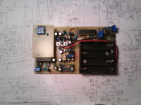
Uses Zener diodes to generate avalanche noise signal, then differential amplifier (and a few analog filters) to eliminate deterministic effects. The noise signal is captured by ATTiny2313 and sent to an FAT32 SD card as a sequence of meaningless hex numbers. I tested random number sequences in MATLAB to check for randomness. I designed and produced a prototype PCB (that you can see in attached photos and PCB layout in .pdf in natural size to check for dimensions. In the same .pdf file there is still unfinished PCB for my nixie-VFD guitar tuner, also in natural size). This RNG is designed with cheap and ubiquitous copmponents and still creates random sequences of good randomness. I tried all the methods that I know to analize the random sequences. If you know more about mathematical methods for checking the randomness of the sequence, you could be interested to check yourself. I have the circuit schematics drawn on paper.
Corrective filter has been added to RNG3 (simplified RNG2 without boost converter, powered by 2x 9V batteries) to equilize frequencies of 8-bit raw random values - this is now RNG4 on perfboard. For easier adjustment of analog filters, a simple spectrum analyser with ATmega8 and 2x16 LCD was designed and tested.
The final version is RNG5, which will be published in Elektor Magazine, together with the accompanying Bit Stream Analyser.
Random numbers are used in applications like cryptography, gaming & gambling (search document for RNG). They can also be used to estimate the value of PI.
Watch this video to learn how to correctly adjust the Random Number Generator.
Project Elements
Discussion (10 comments)

Mutlu Kubilay 4 years ago

lux36 4 years ago
thank you for your interest. You will have to assemble the devices yourself, but the PCBs are still available through the Store:
https://www.elektor.com/random-number-generator-bare-pcb-150116-1
https://www.elektor.com/rng-bit-stream-analyser-bare-pcb-150116-2
If you have any questions regarding assembling/adjusting the devices, don't hesitate to contact me. A device like a cryptographic-grade TRNG can always be improved, so any kind of feedback is useful - every upgraded version of firmware was a result of at least one useful feedback. Good luck!

ElektorLabs 5 years ago

ElektroMaker 8 years ago

lux36 8 years ago
Where exactly would you put it? In place of diff. amp transistors T4 and T5 it would probably improve the response and symmetry of the differential amplifier, but this is not the source of DC offset variation.
Variable DC offset that needs to be automatically compensated happens because of two main reasons:
1.) Operating point and static bias current of T7 transistor slightly change with temperature. This moves AIN0 DC operating point slightly up or down . Moreover, the noise signal at its collector has an amplitude of 0.5-1.0Vpp which is far more than 25-50 mV (what is usually considered as "small signal" on bipolar transistor). This means that output voltage is assymetric around its mean value, so any change of amplification on T7 also directly affects 0/1 ratio.
2.) Ones and zeroes are extracted based on state of MCU's internal comparator. This is an opamp with an offset voltage up to 40 mV, which changes unpredictably with time and temperature. This also needs to be automatically compensated.

Sunil_M 9 years ago
RANDOM NUMBER GENERATION
Introduction:
Using Zener diodes to generate avalanche noise signal, then differential amplifier (and a few analog filters) eliminate deterministic effects. The noise signal is captured by ATTiny2313 and sent to an FAT32 SD card as a sequence of meaningless hex numbers.
This RNG is designed with cheap and ubiquitous components and still creates random sequences of good randomness.
Corrective filter has been added to equalize frequencies of 8-bit raw random values
Hardware:
K1: SD card slot
K2: battery or power connector (18VDC)
K3: Reference signal DC test point
K4: Random bitstream DC test point
K5: ICSP connector
S1: Start switch
S2: Stop Switch
S3: Soft start switch
S4: Megabyte selection switch for RANDOM.HEX file
S5 to S7: corrective filter selection switches
Circuit Description:
The circuit divided in to three major parts as below
Power supply section:
The circuit operates on 18V DC power supply and hence two 9V batteries can be connected in series to power ON the board via connector K2 with polarity as marked on board. Switch S1 is used to switch on the power section momentary by bypassing the power on circuit of T1 and T2 transistors. This action generates the power supply and MCU IC1 start working which then generates the power hold signal on the pin PD1. This signal activates power ON circuitry of T1 and T2 and holds the power ON for circuit after depressing switch S1. Switch S1 need to hold for the movement to start the MCU IC1 (Hardly one or two seconds). Switch S2 is use to stop the power ON stage.
The switched 18V is then fed to IC2 which is a 6V regulator IC for generating 6V. The 18V is also used to generate a 14V DC supply by using IC3 and T3 with preset P1. The output voltage of IC2 is also used to generate 3.3V power supply for MCU and SD card by using IC4 and IC5 which is a 3.3V regulator.
LED4 is indicating power ON status of the circuit and also as battery OK signal. The IC6 and the surrounding components are used for battery monitoring and the output of this is fed to the MCU pin PB2 for checking battery status. Switch S3 is use as a soft start switch for the circuit.
Noise Generation & Amplifier:
Differential amplifier transistor T4, T5 and T6 are responsible for noise generation and noise output is taken out from a differential amplifier transistor T5. Current through each branch of the transistor T4 and T5 is balanced to 1mA by using the preset P3 and current through T6 is kept 2mA by using preset P4. The circuit operates on 6V and 14V supply to generate required noise signal. The generated noise signal is then send to amplifier section.
This section also has corrective a L, C, & R filter. Selection switch S5 is used for determining lower cut off frequency by selecting a different combination of capacitors connected to switch. Transistor T7 is an amplifier and operates on 3.3V supply. Switch S6 used to select different capacitor combination for output signal filter. The DC level of signal can be varied by using preset P5. Switch S7 and preset is the part of filter network used to filter output signal. Output of the amplifier and filter section is then send to analog input of MCU at AIN0 and AIN1 pins.
MCU Section:IC1 ATTiny2313 is the MCU used for performing all the reading, storing and controlling functions. The MCU is interfaced with the SD card using the SPI protocol pins namely MISO,MOSI/SS and clock also connected in parallel to these pins is a four way switch S4 which is used to determine the size of file in megabytes to be created. Three indication LEDS: LED1, LED2 and LED3 are connected to PORTD of the MCU. The function of each LED is as follows:
LED1 – Green LED for indicating initialization complete or writing complete
LED2 – Red LED for error indication
LED3 – Yellow LED indicating card detected and cluster change
To generate a 16MB file S4 must kept all switches in OFF state.
Software:
The software is written in assembly for Attiny2313 using Atmel’s AVR studio 4.
The SPI protocol is used to communicate with the SD card. The software creates a FAT table and writes the random numbers generated into the sectors. The SD card interfacing commands are saved into the internal memory of the MCU.
The system first checks if the SD are inserted and if it finds a card inserted then it sends 74 clock pulses for initializing the card followed by the CDM0 for selecting SPI mode. After which a series of commands have been sent to the SD card. If response is correct then initialization is completed which is indicated by turning ON green led (LED1) (PORTD.4) else it will turn ON the red LED (LED2) (PORTD.3).the entire memory is then flashed. The number of sectors and clusters of the SD card are arranged in a FAT table. Each new cluster created is divided into sectors.
The random numbers are generated on the basis of the ACO bit (analog comparator output) of the ACSR register (PORTD.6) that is connected to the noise and amplification circuitry. The timer is configured in the CTC mode and on every timer compare, the ACO bit is read and written into every sector of the SD card until the user set size of file in megabytes is reached. The LED3 is turned ON every cluster change
The size of the file is determined by reading the switches connected to S4.the switch status is read and is inverted then the value is appended by a 1 so that the value doesn’t be zero at any point. This value is considered to be the maximum size of the file in megabyte. On completion of the write cycles in the SD card the LED1 is turned ON to indicate write complete and a file named ‘RANDOM.HEX’ is created in the DS card
Check for battery (PORTB.2) if ok Write clusters, sectors first FAT table, RANDOM.HEX file
Testing procedure:
- Power up the circuit with a 18VDC
- Set switches of S4 to set the desired size of file
- Connect an SD card in the SD card slot
- Press and hold switch S1 for about 3seconds until LED4 becomes stable
- If the SD card is detected then the LED3 will turn ON.
- if the SD card initializes successfully then LED1 will turn ON
- When writing starts only the LED4 will remain ON and the LED3 will blink occasionally to indicate change of cluster.
- When the writing into the SD completes the LED1 will turn ON
- You can now remove the SD card and read it using your PC
- A file named RANDOM.hex will be created of the desired.
- Note that this file when zipped should remain of the same size a unzipped
150116-random-number-generator-amp-v1-2.jpg (329kb)
150116-random-number-generator-mcu-v1-2.jpg (421kb)
150116-random-number-generator-noise-v1-2.jpg (276kb)
150116-random-number-generator-pss-v1-2.jpg (353kb)
Hardware_1.3.zip (9736kb)
firmware.zip (2357kb)
bom.zip (19kb)
Project Outputs for 150116 Random Number Generator_V1.4.zip (120kb)

lux36 9 years ago

lux36 9 years ago

Sunil_M 9 years ago
RANDOM NUMBER GENERATION
Introduction:
Using Zener diodes to generate avalanche noise signal, then differential amplifier (and a few analog filters) eliminate deterministic effects. The noise signal is captured by ATTiny2313 and sent to an FAT32 SD card as a sequence of meaningless hex numbers.
This RNG is designed with cheap and ubiquitous components and still creates random sequences of good randomness.
Corrective filter has been added to equalize frequencies of 8-bit raw random values
Hardware:
K1: SD card slot
K2: battery or power connector (18VDC)
K3: Reference signal DC test point
K4: Random bitstream DC test point
K5: ICSP connector
S1: Start switch
S2: Stop Switch
S3: Soft start switch
S4: Megabyte selection switch for RANDOM.HEX file
S5 to S7: corrective filter selection switches
Circuit Description:
The circuit divided in to three major parts as below
Power supply section:
The circuit operates on 18V DC power supply and hence two 9V batteries can be connected in series to power ON the board via connector K2 with polarity as marked on board. Switch S1 is used to switch on the power section momentary by bypassing the power on circuit of T1 and T2 transistors. This action generates the power supply and MCU IC1 start working which then generates the power hold signal on the pin PD1. This signal activates power ON circuitry of T1 and T2 and holds the power ON for circuit after depressing switch S1. Switch S1 need to hold for the movement to start the MCU IC1 (Hardly one or two seconds). Switch S2 is use to stop the power ON stage.
The switched 18V is then fed to IC2 which is a 6V regulator IC for generating 6V. The 18V is also used to generate a 14V DC supply by using IC3 and T3 with preset P1. The output voltage of IC2 is also used to generate 3.3V power supply for MCU and SD card by using IC4 and IC5 which is a 3.3V regulator.
LED4 is indicating power ON status of the circuit and also as battery OK signal. The IC6 and the surrounding components are used for battery monitoring and the output of this is fed to the MCU pin PB2 for checking battery status. Switch S3 is use as a soft start switch for the circuit.
Noise Generation & Amplifier:
Differential amplifier transistor T4, T5 and T6 are responsible for noise generation and noise output is taken out from a differential amplifier transistor T5. Current through each branch of the transistor T4 and T5 is balanced to 1mA by using the preset P3 and current through T6 is kept 2mA by using preset P4. The circuit operates on 6V and 14V supply to generate required noise signal. The generated noise signal is then send to amplifier section.
This section also has corrective a L, C, & R filter. Selection switch S5 is used for determining lower cut off frequency by selecting a different combination of capacitors connected to switch. Transistor T7 is an amplifier and operates on 3.3V supply. Switch S6 used to select different capacitor combination for output signal filter. The DC level of signal can be varied by using preset P5. Switch S7 and preset is the part of filter network used to filter output signal. Output of the amplifier and filter section is then send to analog input of MCU at AIN0 and AIN1 pins.
MCU Section:IC1 ATTiny2313 is the MCU used for performing all the reading, storing and controlling functions. The MCU is interfaced with the SD card using the SPI protocol pins namely MISO,MOSI/SS and clock also connected in parallel to these pins is a four way switch S4 which is used to determine the size of file in megabytes to be created. Three indication LEDS: LED1, LED2 and LED3 are connected to PORTD of the MCU. The function of each LED is as follows:
LED1 – Green LED for indicating initialization complete or writing complete
LED2 – Red LED for error indication
LED3 – Yellow LED indicating card detected and cluster change
To generate a 16MB file S4 must kept all switches in OFF state.
Software:
The software is written in assembly for Attiny2313 using Atmel’s AVR studio 4.
The SPI protocol is used to communicate with the SD card. The software creates a FAT table and writes the random numbers generated into the sectors. The SD card interfacing commands are saved into the internal memory of the MCU.
The system first checks if the SD are inserted and if it finds a card inserted then it sends 74 clock pulses for initializing the card followed by the CDM0 for selecting SPI mode. After which a series of commands have been sent to the SD card. If response is correct then initialization is completed which is indicated by turning ON green led (LED1) (PORTD.4) else it will turn ON the red LED (LED2) (PORTD.3).the entire memory is then flashed. The number of sectors and clusters of the SD card are arranged in a FAT table. Each new cluster created is divided into sectors.
The random numbers are generated on the basis of the ACO bit (analog comparator output) of the ACSR register (PORTD.6) that is connected to the noise and amplification circuitry. The timer is configured in the CTC mode and on every timer compare, the ACO bit is read and written into every sector of the SD card until the user set size of file in megabytes is reached. The LED3 is turned ON every cluster change
The size of the file is determined by reading the switches connected to S4.the switch status is read and is inverted then the value is appended by a 1 so that the value doesn’t be zero at any point. This value is considered to be the maximum size of the file in megabyte. On completion of the write cycles in the SD card the LED1 is turned ON to indicate write complete and a file named ‘RANDOM.HEX’ is created in the DS card
Check for battery (PORTB.2) if ok Write clusters, sectors first FAT table, RANDOM.HEX file
Testing procedure:
- Power up the circuit with a 18VDC
- Set switches of S4 to set the desired size of file
- Connect an SD card in the SD card slot
- Press and hold switch S1 for about 3seconds until LED4 becomes stable
- If the SD card is detected then the LED3 will turn ON.
- if the SD card initializes successfully then LED1 will turn ON
- When writing starts only the LED4 will remain ON and the LED3 will blink occasionally to indicate change of cluster.
- When the writing into the SD completes the LED1 will turn ON
- You can now remove the SD card and read it using your PC
- A file named RANDOM.hex will be created of the desired.
- Note that this file when zipped should remain of the same size a unzipped
150116-random-number-generator-amp-v1-1.jpg (329kb)
150116-random-number-generator-mcu-v1-1.jpg (421kb)
150116-random-number-generator-noise-v1-1.jpg (276kb)
150116-random-number-generator-pss-v1-1.jpg (353kb)
Hardware_1.3.zip (9736kb)
firmware.zip (2357kb)
bom.zip (19kb)
Project Outputs for 150116 Random Number Generator_V1.4.zip (120kb)

lux36 9 years ago

lux36 9 years ago

Sunil_M 9 years ago
RANDOM NUMBER GENERATION
Introduction:
Using Zener diodes to generate avalanche noise signal, then differential amplifier (and a few analog filters) eliminate deterministic effects. The noise signal is captured by ATTiny2313 and sent to an FAT32 SD card as a sequence of meaningless hex numbers.
This RNG is designed with cheap and ubiquitous components and still creates random sequences of good randomness.
Corrective filter has been added to equalize frequencies of 8-bit raw random values
Hardware:
K1: SD card slot
K2: battery or power connector (18VDC)
K3: Reference signal DC test point
K4: Random bitstream DC test point
K5: ICSP connector
S1: Start switch
S2: Stop Switch
S3: Soft start switch
S4: Megabyte selection switch for RANDOM.HEX file
S5 to S7: corrective filter selection switches
Circuit Description:
The circuit divided in to three major parts as below
Power supply section:
The circuit operates on 18V DC power supply and hence two 9V batteries can be connected in series to power ON the board via connector K2 with polarity as marked on board. Switch S1 is used to switch on the power section momentary by bypassing the power on circuit of T1 and T2 transistors. This action generates the power supply and MCU IC1 start working which then generates the power hold signal on the pin PD1. This signal activates power ON circuitry of T1 and T2 and holds the power ON for circuit after depressing switch S1. Switch S1 need to hold for the movement to start the MCU IC1 (Hardly one or two seconds). Switch S2 is use to stop the power ON stage.
The switched 18V is then fed to IC2 which is a 6V regulator IC for generating 6V. The 18V is also used to generate a 14V DC supply by using IC3 and T3 with preset P1. The output voltage of IC2 is also used to generate 3.3V power supply for MCU and SD card by using IC4 and IC5 which is a 3.3V regulator.
LED4 is indicating power ON status of the circuit and also as battery OK signal. The IC6 and the surrounding components are used for battery monitoring and the output of this is fed to the MCU pin PB2 for checking battery status. Switch S3 is use as a soft start switch for the circuit.
Noise Generation & Amplifier:
Differential amplifier transistor T4, T5 and T6 are responsible for noise generation and noise output is taken out from a differential amplifier transistor T5. Current through each branch of the transistor T4 and T5 is balanced to 1mA by using the preset P3 and current through T6 is kept 2mA by using preset P4. The circuit operates on 6V and 14V supply to generate required noise signal. The generated noise signal is then send to amplifier section.
This section also has corrective a L, C, & R filter. Selection switch S5 is used for determining lower cut off frequency by selecting a different combination of capacitors connected to switch. Transistor T7 is an amplifier and operates on 3.3V supply. Switch S6 used to select different capacitor combination for output signal filter. The DC level of signal can be varied by using preset P5. Switch S7 and preset is the part of filter network used to filter output signal. Output of the amplifier and filter section is then send to analog input of MCU at AIN0 and AIN1 pins.
MCU Section:IC1 ATTiny2313 is the MCU used for performing all the reading, storing and controlling functions. The MCU is interfaced with the SD card using the SPI protocol pins namely MISO,MOSI/SS and clock also connected in parallel to these pins is a four way switch S4 which is used to determine the size of file in megabytes to be created. Three indication LEDS: LED1, LED2 and LED3 are connected to PORTD of the MCU. The function of each LED is as follows:
LED1 – Green LED for indicating initialization complete or writing complete
LED2 – Red LED for error indication
LED3 – Yellow LED indicating card detected and cluster change
To generate a 16MB file S4 must kept all switches in OFF state.
Software:
The software is written in assembly for Attiny2313 using Atmel’s AVR studio 4.
The SPI protocol is used to communicate with the SD card. The software creates a FAT table and writes the random numbers generated into the sectors. The SD card interfacing commands are saved into the internal memory of the MCU.
The system first checks if the SD are inserted and if it finds a card inserted then it sends 74 clock pulses for initializing the card followed by the CDM0 for selecting SPI mode. After which a series of commands have been sent to the SD card. If response is correct then initialization is completed which is indicated by turning ON green led (LED1) (PORTD.4) else it will turn ON the red LED (LED2) (PORTD.3).the entire memory is then flashed. The number of sectors and clusters of the SD card are arranged in a FAT table. Each new cluster created is divided into sectors.
The random numbers are generated on the basis of the ACO bit (analog comparator output) of the ACSR register (PORTD.6) that is connected to the noise and amplification circuitry. The timer is configured in the CTC mode and on every timer compare, the ACO bit is read and written into every sector of the SD card until the user set size of file in megabytes is reached. The LED3 is turned ON every cluster change
The size of the file is determined by reading the switches connected to S4.the switch status is read and is inverted then the value is appended by a 1 so that the value doesn’t be zero at any point. This value is considered to be the maximum size of the file in megabyte. On completion of the write cycles in the SD card the LED1 is turned ON to indicate write complete and a file named ‘RANDOM.HEX’ is created in the DS card
Check for battery (PORTB.2) if ok Write clusters, sectors first FAT table, RANDOM.HEX file
Testing procedure:
- Power up the circuit with a 18VDC
- Set switches of S4 to set the desired size of file
- Connect an SD card in the SD card slot
- Press and hold switch S1 for about 3seconds until LED4 becomes stable
- If the SD card is detected then the LED3 will turn ON.
- if the SD card initializes successfully then LED1 will turn ON
- When writing starts only the LED4 will remain ON and the LED3 will blink occasionally to indicate change of cluster.
- When the writing into the SD completes the LED1 will turn ON
- You can now remove the SD card and read it using your PC
- A file named RANDOM.hex will be created of the desired.
- Note that this file when zipped should remain of the same size a unzipped
BOM List (19kb)
GERBER File (120kb)
150116-random-number-generator-amp-v1-0.jpg (329kb)
150116-random-number-generator-mcu-v1-0.jpg (421kb)
150116-random-number-generator-noise-v1-0.jpg (276kb)
150116-random-number-generator-pss-v1-0.jpg (353kb)
Hardware_1.3.zip (9736kb)
firmware.zip (2357kb)

lux36 9 years ago

lux36 9 years ago

lux36 9 years ago
PRNG sequence generator, more than 10 different algorithms (82kb)
Sample random sequences, from RNG4 or PRNGs for reference (21390kb)
NIST testing report (13kb)

lux36 9 years ago
After creating a histogram of RANDOM.HEX file generated by RNG2 (the one you had uploaded) , an uneven distribution of different raw hex values (0x0F and 0xF0 3x more frequent than 0x55 and 0xAA) is observed. This is not good, especially for OTP code key. I designed an additional analog filter, added it to RNG3 - this is RNG4, assembled on perfboard, adjusted (with a help of a simple digital bitstream analyser - ATmega8 and 2x16 LCD) and tested. Attached is a RANDOM.HEX generated by RNG4 - compare its histogram with the one generated by RNG2 and you will see an obvious improvement. You can use WINHEX to generate a histogram - very simple.
I attached one more .zip file containing Bode diagram of analog circuit and a simple bitstream analyzer that I used to adjust my RNG4. Frequencies of bit patterns 1f (0x00 or 0xFF), 2f (0x0F or 0xF0), 4f (0x33 or 0xCC) and 8f (0x55 or 0xAA) must be equalized, along with 0/1 ratio (number in upper right corner of LCD - must be trimmed to 511-512). This explains how to adjust the RNG4 to meet NIST criteria. Have fun!
RNG4_frequency_correction_WORD_doc.zip (124kb)
rng4-on-perfboard-0.jpg (269kb)
rng4-with-bitstream-analyser.jpg (402kb)
BitstreamAnalyzerSchematics and Bode diagram of analog section.zip (1007kb)

ClemensValens 9 years ago
We finally gave the board a try and it appears to work fine. Attached is a 16 MB file that the board produced. It is zipped so that it could be uploaded to Elektor.Labs.
Many data compression techniques try to uncorrelate data to reduce its size. When compression is not possible, then the data is not correlated. White noise is uncorrelated. The attached zip file has a compression factor of slightly more than 1 (1.000052632, the zip file of course has some overhead due to the file format), meaning no compression. From this we can conclude that the data has a very low correlation factor and therefore is very random.
Well done :-)
Regards,
Clemens
Updates from the author
lux36 5 years ago
The LEDs are now programmed to flash in the test mode to enable easier adjustment of P5:
-LED3 (yellow) flashing - PWM is higher than 50%
-LED3 off - PWM is lower than 50%
-LED2 (red) flashing- PWM reaches 0% (LED3 off) or 100% (LED3 flashing)
-LED1 (green) flashing- PWM is between 40% and 60% - P5 set correctly
-LED1 on - test mode completed, PWM value OK and written to MCU EEPROM
-LED2 on, LED3 off -test mode completed- P5 setting not good- PWM reaches 0%
-LED2 on, LED3 on -test mode completed- P5 setting not good- PWM reaches 100%
lux36 5 years ago
After all the adjustments of S5,S6 and S7 with help of BSA, the precise trimming of 0/1 can be done by changing the 16-bit value at 0x00AE - increasing this constant increases the number of ones, decreasing it increases the number of zeroes.
For even better NIST testing results!
lux36 5 years ago
However, two other types were tested with good results:
- BZX85C12
- 1N759ATR
Each type has a different frequency specturm, and requires different filter settings, but it is possible to adjust analog filters for both types to get good results to pass the NIST testing.
lux36 6 years ago
Rules to set S5,S6 and S7 after correct setting of RNG P5 and BSA trimmers - all the values f1,f2,f4 and f8 refer to BSA LCD readings:
-if frequencies f1 and f2 are lower than f4 and f8, then the lower corner analog frequency defined by S5 is too high -> increase the S5 capacitance
-if frequencies f1 and f2 are higher than f4 and f8, then the lower corner analog frequency defined by S5 is too low -> decrease the S5 capacitance
-if frequency f2 is higher than f4, then the resonant analog frequency of S6-S7 notch filter is too high -> increase the S6 capacitance
-if frequency f2 is lower than f4, then the resonant analog frequency of S6-S7 notch filter is too low -> decrease the S6 capacitance
-if frequencies f2 and f4 are about equal, but higher than f1 and f8, then the maximum "dip" of S6-S7 notch filter is too low ->decrease the S7 resistance
Please note that is is even possible to achieve correct BSA readings at different S5,S6 and S7 settings, and still pass NIST testing in both versions!
This way every RNG setting will yield a slightly different histogram and your RNG will always have a little bit of your own "touch" in its setting and its random numbers output.
When you get a histogram similar to the one on figure 5 in the Elektor article, it will surely pass the NIST testing.
lux36 6 years ago
lux36 5 years ago
Before you start to adjust the filters, first check the amplitude of signal at T7 collector - the best is with analog oscilloscope. If it is too high, reduce the value of R42 (e.g. put 1kohm trimpot in place of 1.5k fixed resistor). Reducing the R42 will reduce the signal amplitude, but will also move the DC operating point higher up, and this will also keep T7 from going to saturation.
Higher voltage on T7 collector is not a problem because it keeps the Ccb (collector-base) parasitic capacitance low, so the Miller capacitance stays low and this will not spoil the HF. Too low voltage increases Ccb, and smothers the HF.
lux36 8 years ago
One final modification has been done before making the final version that will be published in Elektor - the RNG5. The main problem with RNG4 was that DC offset for threshold (for voltage comparator inside ATTiny2313) had to be trimmed manually (by trimmer preset) and that was sensitive to temperature - opamps have an inherent DC offset that slowly varies. RNG5 has a feedback that automates the DC trimming with PWM output from the MCU. This automatically balances the 0/1 ratio.
A simple method of post-processing of recorded random sequences has been tested with good results. Simply take two random numbers files (RANDOM.HEX) generated by RNG5, and perform on-time pad "encryption" of one of them with the other - a simple bitwise XOR between them. Now you get a RANDOM.HEX file with much flatter histogram (with a variation of only +/- 2%-3%) that passes certain NIST test for much longer sequences - like for example the "Runs" test that now passes smoothly for sequences longer than 500.000 bits, as opposed to 50.000 bits that can be achieved without post-processing.
This one-time pad encryption/decryption was tested on my OTP crypto device, in offline mode, and this device is my next Labs project!