

Wireless SmartProbe
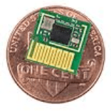
A versatile measuring instrument and data-logger built into a hand-held probe. The instrument has no controls or display instead using a Bluetooth Low Energy (BLE) connection to a smartphone or tablet app.The SmartProbe will have the following components:
A versatile measuring instrument and data-logger built into a hand-held probe. The instrument has no controls or display instead using a Bluetooth Low Energy (BLE) connection to a smartphone or tablet app.
The SmartProbe will have the following components:
- A Cypress EZ-BLE PSoC module. This comprises a BLE radio, a 32-Bit ARM processor, programmable digital logic and highly configurable analog circuits.
- Li-ion Battery Power. A small rechargeable battery enables the probe to work without an external power supply and gives full galvanic isolation "for free".
- An FRAM memory chip for data-logging. This new memory technology is a fully non-volatile RAM avoiding the block writing and limited cycle lifetime of EEPROM.
- USB connection. As well as providing battery charging, this will allow for firmware loading and an alternative to BLE for reading the data-logger. It is not recommended for on-line measurements since it will break galvanic isolation.
The EZ-BLE module has all the active components needed for all but the most sophisticated instruments so the input components will be minimal and mostly passive. Initially it is planned to duplicate the functionality of a typical multimeter, but the probe will be easily adapted and extended to a range of more complex instruments such as LCR meters, transistor testers, frequency counters and even modest bandwidth oscilloscopes.
The app will allow the readings from multiple probes to be integrated to expand to a full data acquisition system.
I have a good deal of practical experience with the EZ-BLE PRoC module from which the PSoC module has been developed. It is very hobbyist friendly as the IDE is free and the USB programming/debugging adapter can be obtained as part of a starter kit for negligable cost. The analog and logic systems are configured using schematics and the BLE from a wizard which makes it easy to use custom BLE profiles rather than having to rely on standard ones provided by the SIG or the manufacturer.
Discussion (3 comments)
JohnHind 9 years ago
These schematics cover all elements of the circuit that are generic and not related to the specific measurement functionality of the SmartProbe. The schematics have been prepared in PSoC Creator using the limited range of annotation symbols and are therefore a little eccentric. In particular nothing is signified by some connections being blue dotted lines and some being solid black lines.
The Digital Infrastructure schematic is very straight forward: just the BLE and RTC (Teal Time Clock) PSoC components and a Serial Communication Block (SCB) in I2C mode to which is connected the FM24V10 FRAM chip. This is a 128k byte Ferroelectric Random Access Memory. It can be written and read just like an SRAM, but is non-volatile like an EEPROM. The I2C bus is also made available for application circuits should they require additional parts not available on the PSoC chip.
The Power Charging and USB Communications schematic required more extensive research and design work. The initial SmartProbe will contain the smallest LiPo battery I could find, a 110mAHr unit 4x15x28mm in size, however I wanted to circuit to be adaptable for larger batteries too. The MicroChip MCP73871 chip is capable of charging at up to 1.8A but can also limit its current demand to 500mA or 100mA to conform to USB 2.1 standards. This current limit applies to the total current drawn through the IN terminal. The chip prioritises the load (on OUT) over charging the battery, so battery charging current is limited to what remains after deducting the load current. The maximum battery charge rate is set by R5 on PROG1. Generally, a LiPo battery should be allowed well over an hour to fully charge from empty, so in this case the charge rate is set at 100mA maximum which is also the minimum guaranteed from a USB 2.1 port. The current limit is set by the logic level on the SEL and PROG2 inputs.
For future-proofing and general sexiness I decided to use the new reversible USB-C connector, but only using the legacy USB 2.1 data lines not the USB3 super-speed lanes. An FTDI FT230XS chip is used to convert the USB 2.1 data connection to logic level asynchronous serial which drives the PSoCs second SCB in UART mode. This chip also has four definable CBUS pins which among other things can be programmed to provide power management signals. CBUS0 (C0) is used as an input to detect the presence of USB power. C1 is programmed as SLEEP#, an output that goes high when there is USB power available and the host is not in sleep mode – this is connected to enable the charger. C3 drives PROG2 – if set high it sets the input current limit to 500mA, if low to 100mA. This should be set to match the power draw configuration settings in the USB descriptor. If set to 500mA the unit will not function on un-powered USB hubs. Finally, the chip supports the BCD standard which is supported by most high power USB chargers except for Apple and indicates that up to 2A is available. C2 is programmed to go high when a BCD charger is detected: if a link is fitted between T2 and T3, this drives the SEL input to the MCP73871 setting the current limit to 1.8A.
Three status inputs from the MCP73871 drive three inputs (with internal pull-up resistors) in the PSoC enabling it to monitor the status of the power system.
USB-C also includes another power standard called PD or power delivery which enables power to be delivered at the same time as USB signalling. This has an active mode which requires a serial communications protocol, but also a passive mode which just requires sensing of a voltage on pin 5 (or pin 8). Optional support for this standard is provided by routing the sensing voltage through to the PSoC ADC from pad T1. In this case it will also be necessary to break the link between T2 and T3 and drive T2 (SEL) from the PSoC, taking it high if and only if the voltage level indicates that 3.0A is available. T3 (BCD) may also be sensed by a PSoC input to support either type of power delivery.
The FT230XS also contains a 3.3V regulator capable of supplying 50mA which is used to drive the PSoC and FRAM chips. If this is not sufficient power for the application circuit, it may provide its own regulator on the PWR_RAW terminal. The voltage here may vary between the battery minimum of around 3.5 volts and the USB maximum of around 5.2 volts.
Finally, an LM4120 band-gap voltage reference IC is used to provide a precision 2.5v reference for the PSoC ADC to allow maximum accuracy to be achieved.
siv-009.png (189kb)
JohnHind 9 years ago
Cypress Semiconductor's PSoC (Programmable System on Chip) microcontrollers have been around for a long time using propriatery 8-bit cores (PSoC 1) or 8051 cores (PSoC 2). More recently Cypress has extended the range with PSoC 4 and PSoC 5 based respectively on 32-Bit ARM Cortex M0 and Cortex M3 cores. The PSoC has always stood out from the microcontroller crowd by featuring on-chip programmable digital logic and a high degree of on-chip routability for analog peripherals backed up by schematic-based design tooling. The latest PSoC 4 development is on-chip support for Bluetooth Smart also known as Bluetooth Low Energy or BLE.
In this project we will be using the very latest PSoC EZ-BLE module, the CYBLE-014008-00. This is a tiny 11x11x1.8mm module with a PSoC 4 chip and all support circuitry including an antenna. At some point we are going to have to grasp the nettle of soldering this to a PCB, but for the moment we can use a low-cost development board, CYBLE-014008-EVAL (£13.32 from Mouser). This is designed to plug into the CY8CKIT-042-BLE baseboard which provides the programming and debug USB adapter, or to use a MiniProg3 adapter. Either of these options are a little expensive, and we can save money by leveraging one of Cypress's prototyping kits which feature a KITPROG USB adapter along with another PSoC chip on a breakout board. Two examples are CY8CKIT-043, which has a non-BLE PSoC 4M chip or CY8CKIT-059, with a PSoC 5LP chip, either of which costs only £6.66. However, avoid the similar looking CY8CKIT-049-41XX or 42XX since these have USB serial bootloader adapters rather than full debug adapters which is much less flexible. The PSoC Creator IDE software is free of charge, so we have everything we need to start development for an outlay of only £20!
To get started, download PSoC Creator 3.3 SP1 from:
http://www.cypress.com/products/psoc-creator-integrated-design-environment-ide
This is sadly Windows only so you will need a Windows computer or Virtual Machine (the benefit is that the IDE is based on the excellent Microsoft Visual Studio rather than the more common, and in my opinion awful, Eclipse). After installing this, plug in the CY8CKIT and its drivers should install automatically. This done, launch PSoC Programmer and, if requested, follow instructions to update the KITPROG firmware. Next separate the two parts of the CY8CKIT board (assuming you are using either the 043 or 059). They are designed to snap apart, but I was more comfortable using a Dremmel. There are two different header pinouts used on various Cypress projects, a 5-Pin 0.1 inch pitch in-line arrangement as used on the CY8CKIT and a 10-Pin dual in line 1mm pitch as used on the BLE evaluation module. To cover both bases I made a two-part link. Firstly, I soldered a short length of 5-core ribbon cable to the KITPROG sub-board and to a 0.1-inch pin socket at the other end. Separating this into four and one socket sections allows the target to be powered from USB or internally self-powered. Soldering pins to the corresponding connector on the target section of the board allows the two parts to be brought back together for working with that target. Next we need an adapter for the BLE target. To make this we need a 2x5 IDC socket and a short length of 10-way 0.5mm pitch ribbon cable. Solder the other end to a 5-way pin header according to the attached schematic. I used this product:
https://sugru.com/
To make custom back-shells for the connections. Sugru is a great product for electronics hobbyists and developers and I always keep a supply in my fridge (it lasts longer that way).
Connect the BLE module to the KITPROG and plug this in to your computer (I find a USB extension cable is easier than trying to plug the KITPROG directly into a USB port). Launch PSoC Creator, select File; New; Project. Click on Target Device and select 'Launch Device Selector' then scroll down to select CYBLE-014008-00. On the next page, select 'Empty Schematic'. Finally select a name and location for the project and press Finish. Navigate to the Source tab on the explorer and double click to open 'main.c' in the source section. Press Shift-F6 to build the project. Now place a breakpoint at line 23 (click to the left of the line number until a red dot appears). Press F5 to debug this code on the target – once the code is downloaded, the program will halt at the first line of code. Press F5 again to resume execution and the program should now stop at the breakpoint. Each time you press F5 it will go round the 'for' loop and stop again at the breakpoint.
Apart from writing code, the other design processes are graphical in approach. The file 'TopDesign.cysch' is used to design analog and digital circuits schematically. You can drag components from the catalog on the right onto the schematic – try this with the BLE component under Communications. Then right click on the component and select 'configure' to set the component up. Try changing the name from 'BLE_1' to simply 'BLE' – there is no point in the number since there can only be one BLE component. Also try dragging an Analog Pin (from Ports and Pins) onto the schematic and in configuration, change its name to something more meaningful and also check the 'External terminal' box. There is also a (somewhat limited) range of 'Off-Chip' components you can add (for documentation purposes). For example try adding a Photo Resistor and a fixed resistor. Then wire them up to the analog input as a potential divider using the 'wire tool'.
The file 'name.cydwr' has two important tabs. The 'Pins' tab is used to assign pins on the schematic to physical pins on the chip. You should see the analog pin you created on the schematic listed in the table to the right. There was a bug in PSoC creator 3.3 at the time of writing triggered if you try to use the Port drop-down list, so instead just type a port in (for example, try 'P1[3]'). The 'analog' tab is where things get really interesting. Re-build the project to see the analog pin assignment made on the Pins tab. You can see lots of juicy analog capabilities here including the ADC, two current DACs and four op-amps which can be routed internally to the ADC. You bring these components into action by adding components to the schematic and wiring them up, but the Analog tab gives a good idea of what is possible. I’ve attached a screenshot in case you are not yet in a position to follow along.
siv-005.png (344kb)
siv-003.png (19kb)
siv-004.png (62kb)
ClemensValens 9 years ago
See here: http://www.aeroscope.io/
Regards,
Clemens
ClemensValens 9 years ago
JohnHind 9 years ago