

Single-phase 1-kilowatt AC Motor Drive
Three-mode design: integral-cycle switching, phase-cut trailing, or phase-cut leading edge.
Gerber file
CAM/CAD data for the PCB referred to in this article is available as a Gerber file. Elektor GREEN and GOLD members can exclusively download these files for free as part of their membership. Gerber files allow a PCB to be produced on an appropriate device available locally, or through an online PCB manufacturing service.
Elektor recommends the Elektor PCB Service service from its business partner Eurocircuits or AISLER as the best services for its own prototypes and volume production.
The use of our Gerber files is provided under a modified Creative Commons license. Creative Commons offers authors, scientists, educators and other creatives the freedom to handle their copyright in a more free way without losing their ownership.
Components
The BOM (Bill of Materials) is the technically exhaustive listing of parts and other hardware items used to produce the working and tested prototype of any Elektor Labs project. The BOM file contains deeper information than the Component List published for the same project in Elektor Magazine. If required the BOM gets updated directly by our lab engineers. As a reader, you can download the list here.
Want to learn more about our BOM list? Read the BOM list article for extra information.
Component list
Component List
photo 191142-014-94
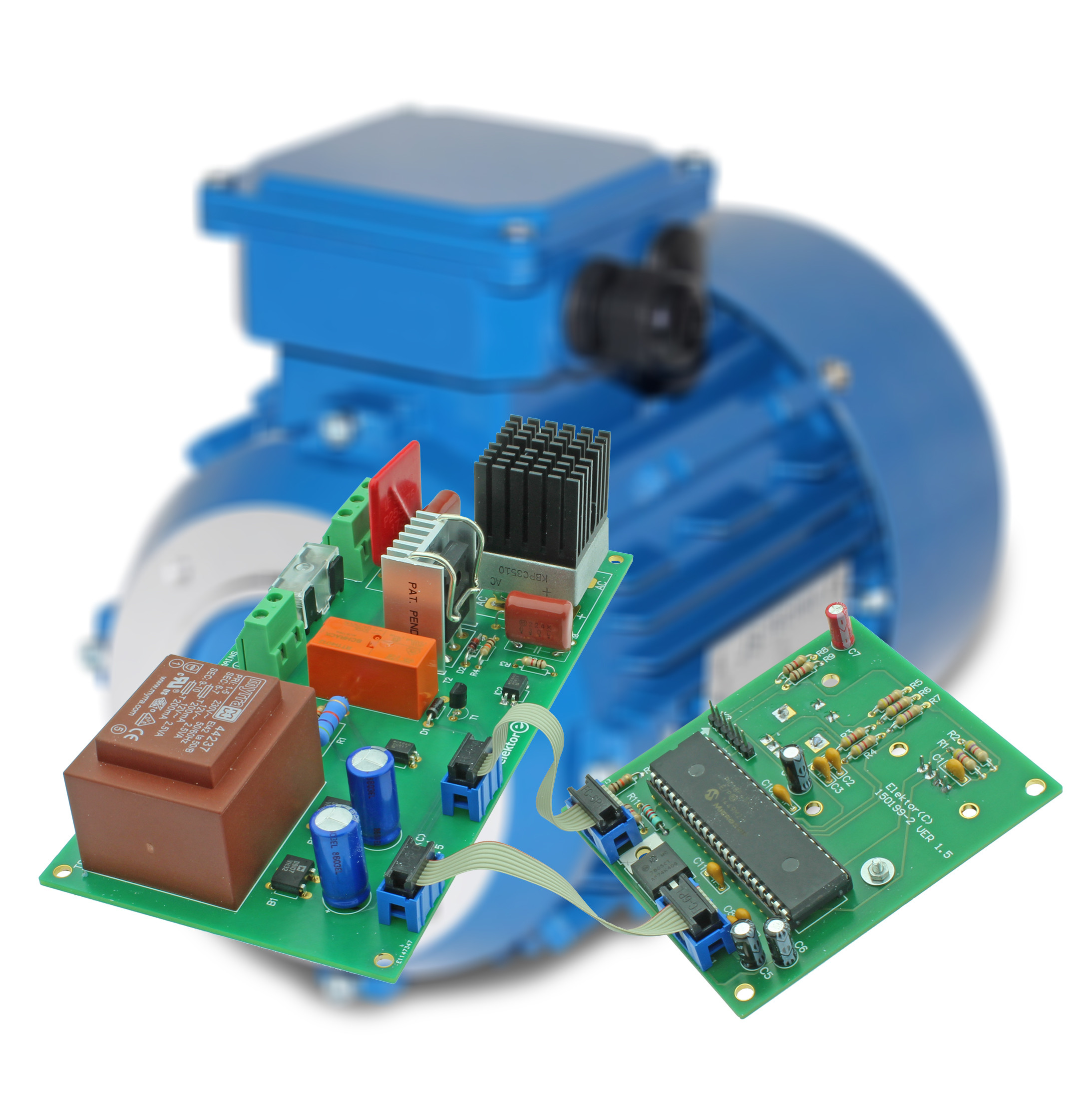
Power electronics board, no. 150199-1
Resistors
R1 = 47kΩ 5%, 3W
R2,R4 = 10kΩ 5%, 250mW, 250V
R3 = 1kΩ 5%, 250mW, 250V
R5 = 2.2kΩ 5%, 2W
R6 = 560Ω 5%, 5W
Capacitors
C1,C2 = 470µF, 50V
C3,C4 = 0.22µF, 630VDC, MPET
Semiconductors
B1,B2,B3 = DB107, 1000V, 1A bridge rectifier
B4 = KBPC3510, 1kV, 35A bridge rectifier
D1 = 1N4007-T
D2 = 1N4742A, 12V, 1W zener diode
IC1,IC2 = PC817X3NSZ1B optocoupler
T1 = BC547B
T2 = STW26NM60N, 20A, 600V, N-Channel MOSFET
Miscellaneous
K1,K3 = 6-way (2x3) boxheader
K2 = 2-way PCB screw terminal block, 0.3’’ (7.62mm) pitch
K4 = 3-way PCB screw terminal block, 0.3’’ (7.62mm) pitch
HS1 = TO-247 heatsink type WV-T247-101E
HS2 = heatsink type 658-60ABT1E (incl. adhesive film)
F1 = 6A(T) (time delay; slow blow), 5x20mm
PCB mount fuse holder, 5x20mm, with cover
RE1 = G2R-14-DC12 (Omron)
TR1 = Power transformer, 2 x 12V, 200 mA, 230V primary, myrra type 44237, Farnell # 1214601
VR1 = V25S275P varistor, 275VAC 470J, 700V clamp, 25mm pitch
PCB 150199-1 v.1.5 from Elektor Store
Component List
2 photos!
191142-015-94 and 191142-018-94
MCU board, no. 150199-2
Resistors
R1-R7 = 4.7kΩ 5%, 250mW, 250V
R8,R9,R10 = 1kΩ 5%, 250mW, 250V
R11 = 3.3kΩ 5%, 250mW, 250V
R12 = 10kΩ 5%, 250mW, 250V
Capacitors
C1,C2,C3,C8-C11 = 0.1µF, 50V
C4,C5,C6 = 10µF 50V, electrolytic
C7 = 1µF 50V, electrolytic
Semiconductors
IC1 = MC7805CTG
IC2 = PIC18F45K22-E/P, programmed, no. 150199-41 from Elektor Store
Miscellaneous
K1,K3 = 6-way (2x3) boxheader
K2 = 6-way SIL pinheader, 0.1’’ pitch
LCD1 = 0.96'' OLED display module, I2C, from Elektor Store, SKU 18747
ENC1 = rotary encoder with pushbutton, Alps EC12E2424407
40-way DIP IC socket, 0.1’’ pitch
Length of 6-way flatcable and 4 IDC connectors for K1,K3 board interconnections
PCB 150199-2 v. 1.5 from Elektor Store
We buy at:

Discussion (0 comments)
Glen W Ruch 5 years ago
The PIC MCU pins 18 and 23 are shown as SCL and SDA. Presumably they are connected to the OLED1 and not shown in the schematic.
Colin Wilson 5 years ago
I noticed this also but, if you look at the PCB it is correctly connected, it's just missing on the diagram.
Glen W Ruch 5 years ago
TheEditor 5 years ago
eduino.io #oetelx 4 years ago
Tthe + / - symbols are correct, but the 4 diodes are pointing the wrong way.
Thanks Glen for pointing this out. I was going to, but you beat me to it ;-)
Jean-Luc Guerlach 5 years ago
TheEditor 5 years ago
Alan Hosler 5 years ago
Michel Greppin 5 years ago
sur la revue, l'afficheur fonctionne correctement mais la sortie reste toujours à 0V et clignote de
temps en temps entre FWD et REV
Geoffroy 4 years ago
The insulation between the two secondary windings seems unknown !!! (The Myrra technical sheet specifies an insulation voltage of 4 kV only between the primary and secondary windings!)
One of the secondary windings of Tr1 is connected to the main, while the other supplies the controller circuit.
Therefore, I think that the controller circuit is insufficiently isolated from the main and must be considered as potentially dangerous.
Cordially
Zinci Sulfati 3 years ago
First the bridge rectifier B4 is reversed on schematics but is OK on circuit board. The ELEKTOR states that only the symbols + (plus) and – (minus) are swapped, but that is not true. To make a correct power board the B4 must be flipped 180 degrees so the plus of the B4 is connected to the drain of T2 and B4 symbols should stay where they are. If it is not flipped the plus of B4 with be connected to MGND which is not correct and will result in a “big bang” and blue smoke if connected to mains.
The IC1 gets its ground in a very strange way at least for me. On power board, from the bridge rectifier B1, the ground goes to pins 1 and 2 of the K1 which then connects to pins 1 and 2 of the K1 on MCU board. From there, through ground pour of the MCU board, the ground goes to pins 4 and 6 of the K3 connector which is then connected to K3 on power board where the pin 3 of the IC1 gets its ground. I do not understand why the ground needed to make such a trip unless it is to prevent ripple of some sort which looks unlikely.
Also SDA and SCL pins on display OLED1 are connected to pins 23 and 18 but are not marked on the other side (R2 and R1).
I
Did anybody made a board on its own?
ElektorLabs 3 years ago
About the ground path you describe: the transistor of IC1 of the PSU board is part of the MCU board, but it is placed on the PSU board because of galvanic isolation. This avoids having mains-connected parts directly connected to the MCU board (like the LED of IC1 of the PSU board).
Zinci Sulfati 3 years ago
I am not arguing about the placement of the IC1 rather the ground via of the power board: pin 3 of the IC1, C1, pins 1&2 of the K1, pins 4&6 of the K3. Instead of connecting it directly (blue line), it goes to MCU (red line) and comes back (yellow line). See the attached photo.
Electrically this does not change anything as it is the same point, but since I am doing the boards myself in EAGLE, and the two boards are separate “entities”, the software complains about not connected via on Power board.
ElektorLabs 3 years ago
jomich 1 year ago
But the power in this mode is very low because at 700W (3A) the varistor VR1 was broken.
And how to calculate and to limit the maximum power for this mode ?