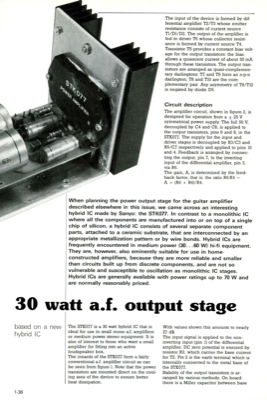
30 watt a.f output stage - based on a new hybrid IC

Continue reading this article with an Elektor Membership.
Join tens of thousands of engineers and electronics enthusiasts worldwide as a
member. Enjoy access to Elektor Magazine, the Elektor library, exclusive discounts,
early notification about Academy Pro products, and more. Select a membership
today and start exploring everything Elektor has to offer. Log in here if you are already a member.

PRINT (Gold)
- 8x Elektor Magazine (Print)
- 8x Elektor Magazine (Digital)
- Integrated Industry Section
- Access to the Elektor Archive*
- Access to over 5,000 Gerber files
- At least 10% Member Discount on Elektor Store*
Free shipping within the US, UK & Ireland.
*Member discount and unlimited archive access only for full GOLD or GREEN members. Trial members have limited access to the online archive.

DIGITAL (Green)
- 8x Elektor Magazine (Print)
- 8x Elektor Magazine (Digital)
- Integrated Industry Section
- Access to the Elektor Archive*
- Access to over 5,000 Gerber files
- At least 10% Member Discount on Elektor Store*
* Member discount and unlimited archive access only for full GOLD or GREEN members. Trial members have limited access to the online archive.


Discussion (0 comments)