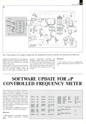
Software Update For Up Controlled Frequency Meter

This is a MEMBER ONLY article. You need a subscription to read this article.
- Unlimited access to online Member Only articles
- 3 new editions Elektor Magazine (digital)
- More than 5000 Gerber files
- 20% member discount on e-books (at elektor.com)
- 10% member discount on Products (at elektor.com)
Available from €5.33 per month.
What is Members Only
Elektor is committed to providing high-quality content on electronics, catering to tens of thousands of paying members. As part of this commitment, Elektor has launched Premium, an initiative that offers exclusive online articles to members sometimes even before they appear in the magazine.
Every day, members can access in-depth articles that showcase the best of Elektor's premium content.
This initiative aims to reward members with early access. Once logged in, members can easily enjoy this exclusive content and engage in discussions about featured projects. While Premium adds to the existing resources available, Elektor will continue to provide a wealth of free information.
Join the Elektor community today to take advantage of Premium and other benefits!


Discussion (0 comments)