

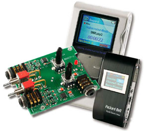
Stereo Microphone Preamplifier
For MP3 equipment
This is a MEMBER ONLY article. You need a subscription to read this article.
- Unlimited access to online Member Only articles
- 3 new editions Elektor Magazine (digital)
- More than 5000 Gerber files
- 20% member discount on e-books (at elektor.com)
- 10% member discount on Products (at elektor.com)
Available from €5.33 per month.
What is Members Only
Elektor is committed to providing high-quality content on electronics, catering to tens of thousands of paying members. As part of this commitment, Elektor has launched Premium, an initiative that offers exclusive online articles to members sometimes even before they appear in the magazine.
Every day, members can access in-depth articles that showcase the best of Elektor's premium content.
This initiative aims to reward members with early access. Once logged in, members can easily enjoy this exclusive content and engage in discussions about featured projects. While Premium adds to the existing resources available, Elektor will continue to provide a wealth of free information.
Join the Elektor community today to take advantage of Premium and other benefits!
Materials
Gerber file
CAM/CAD data for the PCB referred to in this article is available as a Gerber file. Elektor GREEN and GOLD members can exclusively download these files for free as part of their membership. Gerber files allow a PCB to be produced on an appropriate device available locally, or through an online PCB manufacturing service.
Elektor recommends the Elektor PCB Service service from its business partner Eurocircuits or AISLER as the best services for its own prototypes and volume production.
The use of our Gerber files is provided under a modified Creative Commons license. Creative Commons offers authors, scientists, educators and other creatives the freedom to handle their copyright in a more free way without losing their ownership.
Extra info / Update
The indication with connection point ‘C1’ should be moved one level down, i.e., from GND1 down to the same level as C9.
2. On the PCB component overlay, the labels of SMD resistors R29 and R32 have been transposed. Resistor 29 (2 k?) should be the top device in the row of resistors fitted to the right of S1 and S2. R2 (6k?8) should be directly below it.
Component list
R1,R12,R23,R34 = 470?
R2,R24 = 100?
R3,R33 = 4M?7
R4,R5,R25,R26 = 3k?3
R6,R11,R27,R32 = 6k?8
R7,R10,R28,R31,R45,R46 = 47k?
R8,R9,R29,R30 = 2k?
R13,R35 = 33?
R14,R22,R36,R44 = 220k?
R15,R37 = 2k?2
R16 à R19,R38-R41 = 22?
R20,R21,R42,R43 = 10k?
P1,P2 = potentiometer 10k? B Alps type RK09K11310KB (Farnell # 119-1725)
Capacitors
(all SMD):
C1,C4,C6,C7,C8,C10,C13,C15,C16,C17,C19-C22 = 10µF 16 V tantalum, Vishay Sprague 595D106X9016B2T (Farnell # 392-8895)
C2,C3,C5,C9,C11,C12,C14,C18 = 470nF/25 V tantalum, Vishay Sprague 595D474X9025T2T (Farnell # 116-6814)
Semiconductors
D1 = LED, 3mm, red
T1-T8 = BC856ALT1G, SMD, SOT-23, ON Semiconductor (Farnell # 114-7782)
T9,T10 = 2N7002, MOSFET, SMD, SOIC, Texas Instruments (Farnell # 102-1754)
IC1,IC2 = TL071CD, SMD, SOIC, Texas Instruments (Farnell # 958-9449)
Miscellaneous
K1,K2,K3 = 3.5mm jack socket with 3 contacts, Schurter R36310000 (Farnell # 149-933)
S1,S2 = SPST switch, angled pins, PCB mount, height = 12.7mm, C&K 7103MD9 AV2BE (Farnell # 957-5510)
BT1 = 9V battery with clip-on lead
K4 = 2-way PCB pinheader
Case with battery compartment, e.g. BC2, Farnell # 223-554
PCB, ref. 060237-I from ThePCBShop
Discussion (0 comments)
Emil Almberg 4 years ago
The indication with connection point ‘C1’ should be moved one level down, i.e., from GND1 down to the same level as C9.
Thanks.
MarcelC 4 years ago
I am the author of the article. Where did you read this citat? I don't understand without giving me the context, the article is old ...
Marcel CREMMEL
Emil Almberg 4 years ago
The drawing is apparently wrong in 2 places.
By the way, do you think I should build this design today?
It has the advantage of not using expensive special components but maybe there are better solutions today?
I'm interested in building good audio equipment myself, just because it's fun.
MarcelC 4 years ago
The technician who drew the diagram made a mistake in the positioning of the equipotential bonding identifier C1 (see diagram extract). "C1" is the name of the equipotential connected to the "+" input of IC1.
Already at the time of the publication of the article, there were high-performance integrated circuits to make a microphone preamplifier.
But, as an electronics enthusiast like you, I was motivated by achieving similar, if not better, results with "drawer bottom components".
You can have fun changing transistors and analyzing the results ...
Emil Almberg 4 years ago
But I do not understand, can we draw a little so everyone is involved?
See my sketch, according to Elektor, the microphone's inputs should be connected to the transistor's base connections, is that correct?
Also, there's something wrong with the opamp's non-inverted input, where I get lost.
Can you please draw how it should be, thank you!
Again, I do this just because it's fun and of course you want solutions that you can play a lot with, and avoid special circuits!
MarcelC 4 years ago
In view of the many errors in copying the diagram, the easiest way is to provide you with my original schematic.
Note that the PCB conforms to this schematic. There is no scratch track!
Kind regards
Emil Almberg 4 years ago
This rase the old question, is any article in the magazine E really completely flawless?
Thinking about changing your design a bit, I want to remove shutdown via microphone connector, as I do not need that feature, and add a low battery indicator.