

1 Pin uC Interface for HD44780 (and compatible) LC Displays [130397-I]
Almost ervery developer faces one day the situation that his (or her) uC project grows and finally runs out of port pins. In this case there are basically two possible solutions feasible. Either take a bigger uC or use some kind of port expander. If one would like to avoid a bigger uC you have a large number of solutions for port expanding on the market.
Almost ervery developer faces one day the situation that his (or her) uC project grows and finally runs out of port pins. In this case there are basically two possible solutions feasible. Either take a bigger uC or use some kind of port expander. If one would like to avoid a bigger uC you have a large number of solutions for port expanding on the market. The most common ones are shift registers using I2C or SPI interface, giving you the choice between flexibility of I2C, but expensive and slow and SPI, which is fast and simple, but less flexible and needs even one more port pin than I2C. Any case, it costs you 2 or 3 pins to drive your periherial like a HD44780 LCD.
Now my idea was, to drive such a LCD to use a simple HC595 shift register with SPI interface, but wanted to spend for it only a single port pin of the uC. It's clear that this is not breaking any speed records compared to a 8 bit parallel interface, but in contrary to other solutions already existing, data transfer is fast and simple enough to write text and pseudo graphics (via custom characters) on the LCD faster that you can notice. The chosen chip is a 74HC595 with a hand full of cheap components that make up a smart and simple to drive 4 Bit interface for the very popular 2x16 Character LCD Modules or any other LCD using the legendary Hitachi HD44780 or a compatible controller. Of course other format LCDs do work as well as long as they support the 4 Bit Hitachi Mode as most do. As the LCD module at least requires in addition to the 4 data line some control lines like E and RS (R/W tied to ground) and the shift register has 8 data lines, 2 of them are free for other usage, like switching of back light illumination or the like. The basic idea of driving the shift register is to connect the uC port pin to the DS data input via a RC low pass filter and directly also to the SCK shift register clock input. The clock input is edge triggered (rising edge only) and if an idle high level is used, a short low pulse will trigger the shift clock when rising, but the RC at the data input DS didn't have enough time to fall to a low level, so that a logic high gets shifted in. In case the low pulse is long enough for the RC to reach (almost) low level the rising edge of the port pin shifts in a 0.
Some readers might state now that this is not a new principle and so far they're right. It is used in a similar way for such purpose for example by Roman Black and he discribes it on his Web page www.romanblack.com/shift1.htm in detail. (He states, that the principle of using a RC filter to separate short from longer pulses is not new and he didn't invent it, just found the idea somewhere in the Web, and doesn't know who did. Neither do I.)
In his solution he uses a 2nd RC with a 20 times longer time to trigger the latch register to output the data at the pins.
That has two significant disadvantages my solution avoids.
First, as the E input of the LCD needs to see a positive pulse to carry over the 4 data lines and RS state, one has to send the same data twice to create an E pulse, that is, 2 times shift each logic one in of 1us (plus a longer recovery time for the RC, e.g. 15us) and zero of 15us (plus a longer recovery time for the RC, e.g. 30us) followed after 8 shifted bits by a latch pulse of 200us (plus 300us recovery). That really sums up and slows transfer down as an 8 bit wide command in two 4 bit steps takes 3.2ms worst case.
Second, not to forget to mention that in his solution the last bit (Q0) that is shifted in is not usable as it is always 0, leaving only 6 interface pins and 1 spare pin for other use.
The impovement now is to use a different way to carry over the data from the shift register to the data register and to automatically generate the E pulse for the LCD to carry over the output data in a single step without sacrifying any of the data bits. The idea in detail is to use the Q7' direct output of the shift register to trigger the output latch register to carry over automatically the shifted data to the output pins. Of course, that would mean that the first bit for Q7 to be shifted in has to be always a logic 1. I.e. as soon as the last bit for Q0 gets shifted in a 1 (rising edge) at Q7' pin occurs and as it is connected to STCP, the store or latch register input, the data immediately occur at the output pins Q0 to Q7.
To clear the shift register, a second RC with a timing value of T2 >= 20*T1 is used to trigger the MR reset input. A speciality of the 595 chip is, that the MR reset only clears the shift register, but not the latch register for the output pins. So Q7' pin gets cleared to 0 but Q0 to Q7 remain unchanged. This falling edge of Q7' is used to trigger a small simple Monoflop made out of a BS170 MOSFET two resistors and a capacitor to generate the E pulse as soon as the (internal) register of the HC595 gets cleared. Immediately after the recovery time of the long second RC the next data can be transfered to the LCD. The timings I tried out with an Arduino sums up to 1.3ms worst case for a 8 bit data transfer to a LCD, assuming all bits are 0, which is not an legal command the LCD would understand. I wrote a simple Arduino code which is easy to port to other platforms or to be used in own applications. See schematic diagram that makes it more clear how this works.
Questions welcome (German or English language, please).
Discussion (4 comments)
Lucky 10 years ago
After correcting the IF-statement in my earlier contribution, I added a trigger signal to the software to make it easier to get a steady signal on an oscilloscope.
Arduino Digital 9 goes low when the firmware starts sending text to the LCD, and goes high again after every character sent. This yields a nice scope picture, illustrating how this circuit works.
The bottom trace (yellow) shows the signal generated by the Arduino. The small, needle shaped pulses represent logic '1' databits, the longer pulses (approx. 10usec) logic '0'-s. The wide, 200usec pulse resets the 74HC595 shift register. This signal clocks the shift register. NOTE: not all '1'-s are visible in this picture due to limited resolution of the oscilloscope screen!
Although the circuit works with the R1/C1 and R2/C2 values used in the original schematic, I changed both C1 and C2 to 2.2nF (i.e. less than halve the original) in order to lower the bottom voltage levels of the filtered pulses. In particular the reset signal was a bit slow, with the minimal voltage level around 1 to 1.5V. The circuit does work with the original dimensioning though!
The purple trace is the signal on the serial data input (pin 14) of the shift register. The short pulses (logic '1') are filtered out by R1/C1, serial input is low when the shift register is clocked.
The blue trace represents the shift register reset signal (pin 10), the data bit pulses hardly have any influence after filtering by R2/C2.
Last but not least, the green trace is the (pin 12) signal that clocks the output register of the 74HC595, i.e. copies the contents of the shift register to the Qx outputs after eight databits are received. This also triggers the LCD enable signal via C3/T1.
scr07.jpg (68kb)
DE172394 10 years ago
Detlef 10 years ago
Lucky 10 years ago
There is an error in the original sketch. In 'shift595' there's an if-statement:
if (data & i == 0)
which always is false. In this syntax every data bit will be interpreted as a logic '1'. The correct syntax should be:
if ((data & i) == 0)
And YES!!!! Now it works ;-)
Lucky 10 years ago
NECV20 10 years ago
Very well done Goofo,
I like it very much for my LPC800 mini-board, because there so few pins available on a LPC810.
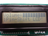
So I ported your Arduino software to the LPC800 system. And quess what: it worked right away! As you can see at the photo.
I add the software to this contribution.
For those who are interested in using this software I have two remarks.
1. To select the only PIO0_x pin needed (if you do not want to use PIO0_3) you should alter the #defines in LCD1wire.h P_OUT, P_OUT_CLR and P_OUT_SET to the approppriate pin (1 for PIO0_0, 2 for PIO0_1, 4 for PIO0_2, ...).
2. The function shift595 is 'time-critical' and may not be interrupted. You will find disabling and renenabling IRQ calls in this function, which are not in the original function by Goofo.
LPCXpresso projectfiles for 1wire LCD (2210kb)
Detlef 10 years ago
NECV20 10 years ago