BotFactory Releases new Multilayer Capability
on

The R&D team at BotFactory has been hard at work for the last couple of years. In October 2015 they introduced a new ink, called “Advanced Ink”, which allowed users to print flexible and rigid circuits on a variety of substrates - FR4 and Kapton included - and this upgrade strengthened their position in the educational market and pushed them into research and development labs at companies in different markets.
As of today, we are announcing our new insulating ink that would enable existing and future users of their desktop PCB factory - Squink - to print and assemble multi-layer boards, deepening on their promise of affordable rapid-prototyping.
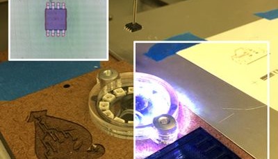
How does it work? Well, it's actually fairly straightfoward. If you have the Squink Complete Set, or have a Squink and have bought our Multilayer Package, you will see that there is a new cartridge containing insulating ink and a curing lamp. The latter is placed on top of the circuit to cure the insulating ink via UV light while protecting the eyes and skin of the users during the process.
The specially-formulated ink is electrically insulating and is compatible with the existing Advanced Ink, allowing users to print insulating ink on top of the conductive traces or to print traces on top of an insulating layer. It can also be used to improve printing on materials that are not easily compatible with the advanced ink like porous, stretchable or textile materials. Application of an additional layer of insulating ink on top of the the upper conductive layer is also an option to protect the exposed traces.
What can I do with Squink now?
Users of the Multilayer Package will be able to design their multi-layered circuits using standard CAD tools like Eagle, Altium or KiCad. Squink will use the exported GERBER files to design the printing strategy and guarantee connection between different layers using stacked VIAS. BotFactory is officially supporting two-layer boards and encourages users to experiment with additional layers. It is likely that official support for additional layers will become available in the near future.
Given the complexity of existing ICs and the growing demand for smaller footprints when it comes to electronic devices, multilayering is mandatory. The introduction of the multilayer capability, even for flexible circuits, will immediately alleviate prototyping pains in applications like Wearables devices, Internet of things, Medical devices, Education, Avionics and Art-tech amongst others.


Discussion (0 comments)