

Circuit Shorts: Print Is Not Dead
April 29, 2021
on
on

When we design circuit boards, we view them in extreme zoom and it’s hard to keep the actual scale in mind. And we’ve all experienced “blind spots” after staring at them for a long time. I’ve developed a process that brings back the scale to my mind and helps me discover problems. I print the design twice when I think it’s ready to be manufactured.
Print #1 is for finding functional issues. I sit somewhere away from my computer with that print, the printed schematic, and highlighter pens and trace every track and tick it off on both documents. It allows me to catch tracks going where they shouldn’t, and also notice microcontroller pads with no connection: a red flag.
I use Print #2 to get the scale back to the fore and to verify the footprints. I do my best to have samples of all the components at this stage. I verify all of them because you never know. But first I measure that “large feature” in both X and Y dimensions. This is important because of annoyingly covert printer scaling; measuring that feature lets me know that I’m indeed working with a true 1:1 print.
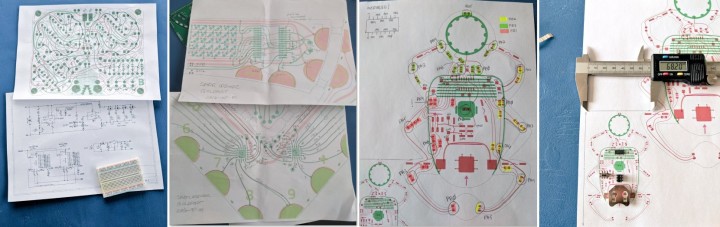
For extra assurance, I ask another person, if one is around and willing, to go through the same process with my design. Another set of eyes for some sanity-checks and questions is a good thing.
The process of setting everything up can be annoying, but it sure ain’t as annoying as getting a board back with the wrong footprint! I also don’t like printing waste — both prints can be on the same piece of paper — but if it means avoiding a scrapped board rev, I think it’s probably worth it.
What techniques do you use to make sure everything is as correct as possible with your PCB before pressing the button for manufacturing?
- Print #1: A scaled-up version of the design, to A4 or A3 paper size, with only the outline and copper features, nothing else. Every physical layer gets its own distinct color with some opacity so that I can see the overlaps between layers.
- Print #2: One-to-one scale print in black with the outline, footprint pads (but not the routing!), and a large feature with a known size in both the X and Y directions. (I use my outline dimension arrows.)
Print #1 is for finding functional issues. I sit somewhere away from my computer with that print, the printed schematic, and highlighter pens and trace every track and tick it off on both documents. It allows me to catch tracks going where they shouldn’t, and also notice microcontroller pads with no connection: a red flag.
I use Print #2 to get the scale back to the fore and to verify the footprints. I do my best to have samples of all the components at this stage. I verify all of them because you never know. But first I measure that “large feature” in both X and Y dimensions. This is important because of annoyingly covert printer scaling; measuring that feature lets me know that I’m indeed working with a true 1:1 print.
For extra assurance, I ask another person, if one is around and willing, to go through the same process with my design. Another set of eyes for some sanity-checks and questions is a good thing.
The process of setting everything up can be annoying, but it sure ain’t as annoying as getting a board back with the wrong footprint! I also don’t like printing waste — both prints can be on the same piece of paper — but if it means avoiding a scrapped board rev, I think it’s probably worth it.
What techniques do you use to make sure everything is as correct as possible with your PCB before pressing the button for manufacturing?
Additional Resources About Circuit Design
Interested in circuit design, PCBs, and related topics? Check out these articles and links.- F. Schaffer, “Simulate Circuits Online: Circuit Simulation Made Simple," ElektorMagazine.com, January 20, 2021.
- C. Valens, "How-To Calculate the Prospective Short-Circuit Current or PSCC," ElektorMagazine.com, March 12, 2020.
- Subscribe to the "Circuit Shorts" tag to receive updates when new articles are posted.
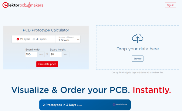
- Looking for eco-friendly and affordable rapid prototyping solution? Check out ElektorPCB4Makers. You can received two PCB prototypes in just three working days!
Read full article
Hide full article
Discussion (1 comment)
RoV 3 years ago
I also print the schematics to double-check them, while for the PCB traces I rely on the DRC check of the CAD, which not only catches wrong or missing connections, but also makes sure that pads and overlay prints do not overlap. I also prefer the CAD to check track sizes for high-current connections and for shapes/cutouts of power plane layers or polygons. I find confusing to do the same on paper: on CAD you can easily turn on/off layers, or keep one layer more visible than the others.
One thing I find useful is displaying top and then bottom overlay layers alone, with tracks and pads grayed, to appreciate defects in text position/orientation/size.
Another thing I find useful, although very time consuming, is having 3D models for each part, because 3D views of the PCB help finding a lot of problems.