

High voltage supply scheme with a simple series regulation for + and - HV
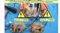
Combining state-of-the art HV Mosfets with a photodiode array optocoupler allows for a simple linear series regulated high voltage supply. The proof-of-pronciple setup covers the ranges for 0..+1400V and 0..-1400V with the ability to supply several 100 microAmperes. The residual rms ripple/noise is < 100mV.
To prepare for a project to build a general purpose high accuracy high-voltage supply suitable various experiments I wanted to explore the possibilities to make a simple to build high voltage (1.5kV) series regulator that works for both polarities.
The presented project addresses this challenge using state-of-the art HV-Mosfets and a not-so-common optocoupler as essential ingredients. Using these, the rest of the regulation circuitry is straightforward and simple.
In order to make a simple low-noise high voltage supply for some experiments with photomultipliers and other radiation detectors I grabbed some parts that were laying around (2 print transformers 230/9V, 6VA, a bunch of 10mF/450V capacitors and 1N4007 diodes). This is enough to experimentally create the raw HV voltages in the range of ±1600V. For stabilization and control using a MOS-FET as series voltage regulator, two dedicated special modern components had to be purchased: a 1700V SIC-Mosfet (MSC750SMA170B, ~5Eur) and a optocoupler (TLP3905, ~1 Eur) that supplies the voltage from a series array of photodiodes as output (up to 7V) that is able to directly drive the MOS_FET. These two latter make the rest of the schematics quite simple and safe.
The corresponding regulation allows to setup positive and negative (using two branches) voltages for 0 to about 1400V (max 0.5mA) with a residual noise floor < 100mV rms.
More details and results arre described in the attached file: HV_regulated_supply1.pdf.
More details and results arre described in the attached file: HV_regulated_supply1.pdf.
Discussion (7 comments)
cvdo 7 months ago
Well, that is indeed a concern, because as is, the voltage over e.g. C5 will rise to 230V×√2×2=650V, well over its specified 450V maximum!
Indeed I'm curious how a resistor would have helped solve this problem
monk99 7 months ago
This of course is not very elegant. Using larger transformers one either must adapt the R values or better use two 450V capacitors in series with load parallel distributiion resistors, which then can be a bit larger but must provide a reasonably fast discharge path.
At the end the shown contraption was intended as a test for the regulation scheme with the unconventional optocoupler as a preparation for a project to build a more elaborqate HV supply wiith a dedicated HV transformer.
Anyway, it is good that you highlighted this point again and put emphasis to the fact that one has to take care not to overload the capacitors!
Corneliu Donciu 8 months ago
Ref. to HV_schematics_corr2, I think that the left terminal of R16 and the + terminal of C9 should be tied to terminal 1 of transformer T2.
JLM7174 8 months ago
https://www.worldradiohistory.com/UK/Wireless-World/90s/Electronic-World-1997-07.pdf
Robert Frisbee 8 months ago
monk99 8 months ago
I will edit the schemtic accordingly.
CerealKiller 8 months ago
CerealKiller 8 months ago
monk99 8 months ago
I upload a corrected schematics.
Deltor 8 months ago
The left lead of R11 should be connected to the anode if D1, respectively GND.
Here I just detected some other weirdness.
The values of R1 ... - each 840kOhm - don't belong to any E-series, the nearest value would be 820kOhm.
Is this some sort of plagiarism protection?
Q: by 1meg you mean 1M - why don't you use an upper case 'M'?
John Walker 8 months ago
I have 2 questions about the circuit:
- is t not more save to use 2 more TLP3905 couplers for the SENSE+ and SENSE- for a strict (optical) separation between the HV and LV circuits?
- The V+ and V- power-supply in the OP-AMP circuit, where they came from ?
monk99 8 months ago
The V+ and V- volatges for the regulation are made useing two diodes and electrolyte capacitors connected to the intermediate 9V winding of the transformer pair (see schematics). In my present proff of principle realisation they have not further regulation.
Note that this topology may have issues with a somewhat too high current in the intermediate branch (see description).
This latter solution comes mainly from the fact that had these transformers layinng around, more adapted solution may use a single transformer with one high voltage and one 6-12V windings, e.g. some tube radio style one.
jost 8 months ago