Wafer pooling: low-cost prototyping service for ICs
November 16, 2015
on
on
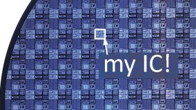
 The Full Service Foundry division of ams AG announced its fast and cost-efficient IC prototyping service, known as Multi-Project Wafer (MPW) or shuttle run. The prototyping service combines several designs from different customers onto a single wafer to offer significant cost advantages as the costs for wafers and masks are shared among a number of different participants.
Multi-Project wafers will not be baked every day, for 2016 the manufacturer has scheduled some 150 MPW runs. Several technologies are available, allowing 1.8V, 5V, 20V and 50V devices. The 0.35µm specialty processes allow for 20V, 50V and 120V devices as well as truly voltage scalable transistors.
All process technologies are supported by the so-called "hitkit", a design kit based on Cadence, Mentor Graphics or Keysight ADS design environments. The hitkit comes complete with fully silicon-qualified standard cells, periphery cells and general purpose analog cells such as comparators, operational amplifiers, low power A/D and D/A converters.
Read full article
Hide full article


Discussion (0 comments)